|
SMX L4812 VERY LOW DROPOUT VOLTAGE REGULATORS same as ST Microelectronics L4812, ST Microelectronics L4808-L4810-L4812, ST Microelectronics L4812, ST Microelectronics L4812CV, ST Microelectronics L4812CX manufactured by Semiconix Semiconductor - Gold chip technology for known good die, flip chip, bare die, wafer foundry for discrete semiconductors, integrated circuits and integrated passive components from Semiconix Semiconductor - Goldchip technology is trademark of Semiconix Corporation for known good die, flip chip, bare die, wafer foundry for discrete semiconductors, integrated circuits and integrated passive components manufactured by Semiconix Semiconductor. Gold metallization for interconnections instead of aluminum or copper, for high reliability devices for system in package applications using silicon printed circuit boards, ceramic substrates or chip on board, assembled via flip chip or chip and wire.
ST Microelectronics L4808-L4810-L4812
SMX L4812 VERY LOW DROPOUT VOLTAGE REGULATORS same as ST Microelectronics L4812, ST Microelectronics L4808-L4810-L4812, ST
Microelectronics L4812, ST Microelectronics L4812CV, ST Microelectronics L4812CX manufactured by Semiconix Semiconductor - Gold chip
technology for known good die, flip chip, bare die, wafer foundry for discrete semiconductors, integrated circuits and integrated passive
components from Semiconix Semiconductor - Goldchip technology is trademark of Semiconix Corporation for known good die, flip chip, bare
die, wafer foundry for discrete semiconductors, integrated circuits and integrated passive components manufactured by Semiconix
Semiconductor. Gold metallization for interconnections instead of aluminum or copper, for high reliability devices for system in package
applications using silicon printed circuit boards, ceramic substrates or chip on board, assembled via flip chip or chip and wire. ST
Microelectronics L4808-L4810-L4812 REGISTER-LOGIN PRODUCTS CROSS REFERENCE /cgi-bin/stock.pl?part=L4812">INVENTORY
/cgi-bin/rfq.cgi?site=4&rows=1&item_1=SMXL4812&c_item_1=">REQUEST QUOTE smxrootwww.semiconix.com/cgi-bin/order.cgi?site=">ORDER ONLINE SITE
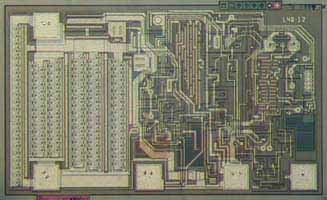
MAP semiconix semiconductor - where the future is today - gold chip technology SMX L4812 - BARE DIE GOLD CHIP TECHNOLOGY™ VERY LOW DROPOUT
VOLTAGE REGULATORS FEATURES APPLICATIONS LDO VOLTAGE REGULATOR Input/Output Typ. 0.4V 400mA Output Current Low Quiescent Current Reverse
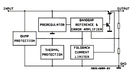
Polarity Protection Over Voltage Protection (±60V) Foldback Current Limiting Thermall Shutdown In DIE form, this device is an excellent
selection for many chip and wire HYBRID CIRCUITS L4812 L4812 VERY LOW DROPOUT VOLTAGE REGULATORS SMXL4812 VERY LOW DROPOUT VOLTAGE
REGULATORS - PRODUCT DESCRIPTION The SMX L4812 series devices are voltage regulator with a very low voltage drop ( typically 0.4 V at
fullrated current), output current up to 400mA, low current and comprehensive on-chip protection. The-quiescentse devices are protected
against load dump and field decay transients of ±60V, polarity reversal and overheating. A foldback current limiter protects against load
short circuits. Available in 5V, 8.5V 9.2V, 10V and 12V versions ( all ±4%, TI = 25°C ) the-quiescentse regulators are designed for
automotive, industrial and consumer applications where low consumption is particularly important. HIGH RELIABILITY BARE DIE AND SYSTEM IN
PACKAGE - SHORT APPLICATION NOTE COB (Chip on Board) and SiP (System-in-Package) are integrating proven mature products in bare die of
mixed technologies i.e. Si, GaAs, GaN, InP, passive components, etc that cannot be easily implemented in SOC (System-on-Chip) technology.
COB and SiP have small size footprint, high density, shorter design cycle time, easier to redesign and rework, use simpler and less
expensive assembly process. For extreme applications the bare die has to withstand also harsh environmental conditions without the
protection of a package. KGD, Known Good Die concept is no longer satisfactory if the die cannot withstand harsh environmental conditions
and degrades. Standard semiconductor devices supplied by many manufacturers in bare die are build with exposed aluminum pads that are
extremely sensitive to moisture and corrosive components of the atmosphere. Semiconix has reengineered industry standard products and now
offers known good die for bare die applications with gold interconnection and well-engineered materials that further enhance the die
reliability. Semiconix also offers Silicon Printed Circuit Board technology with integrated passive components as a complete high
reliability SIP solution for medical, military and space applications. See AN-SMX-001 SEMICONDUCTOR INTEGRATED CIRCUITS MANUFACTURING
PROCESS Semiconductor Integrated Circuits are manufactured using Semiconix in house high reliability semiconductor manufacturing processes.
All semiconductor devices employ precision doping via ion implantation, silicon nitride junction passivation, platinum silicided contacts
and gold interconnect metallization for best performance and reliability. MNOS capacitors, Tantalum Nitride TaN or Sichrome SiCr thin film
resistors are easily integrated with other semiconductor devices on same chip to obtain standard and custom complex device solutions.
SCHEMATIC DIAGRAM L4812 ST Microelectronics L4812 VERY LOW DROPOUT VOLTAGE REGULATORS L4812 MAXIMUM RATINGS PARAMETER SYMBOL VALUE UNITS DC
Input Voltage Vin 35 V DC Input Reverse Voltage Vir -18 V Transient Input Overvoltages LoadDump: 5ms =< Trise =<10ms, tf Fall Time Constant
= 100ms, Rsource =< 0.5 FieldDecay: 5ms =< Tfall =< 10ms,Rsource =< 10 tr Rise Time Constant = 33ms 60 -60 V Junction and Storage
Temperature Range Tj, Tstg -55 to +150 °C ONLY Proper die handling equipment and procedures should be employed. Stresses beyond listed
absolute maximum ratings may cause permanent damage to the device. L4812 ELECTRICAL CHARACTERISTIC VI=14.4V;CO=100F;Tj=25°C unless
otherwise specified. PARAMETER TEST CONDITIONS SYMBOL MIN TYP LIMIT UNITS Output Voltage IO=5mA to 400mA VO 8.83 9.2 9.57 V Operating Input
Voltage VI 26 V Line Regulation VI=13 to 26V; IO=5mA ΔVO/VO 1 10 mV/V Load Regulation IO= 5 to 400mA* ΔVO/VO 3 15 mV/V Dropout Voltage IL =
150mA IL = 400mA* VI-VO 0.2 0.4 0.4 0.7 V QuiescentCurrent IL = 0mA IL = 150mA IL = 400mA * Iq 0.8 25 65 2 45 90 mA mA mA Temperature
Output Voltage Drift ΔVO/ΔT*VO 0.1 mV/°C*V Supply Voltage Rejection IO=350mA;f=320Hz; CO=100F;VI=VO+3V+2Vpp SVR 60 dB Maximum Output
Current IO 800 mA Output Short Circuit Current (fold back condition) ISC 350 500 mA VI=14.4V;CO=100F;Tj=-40to125°C (note1) unless otherwise
specified. PARAMETER TEST CONDITIONS SYMBOL MIN TYP LIMIT UNITS Output Voltage IO=5mA to 400mA VO 8.65 9.2 9.75 V Operating Input Voltage
Note 2 VI 26 V Line Regulation VI=13 to 26V; IO=5mA ΔVO/VO 2 15 mV/V Load Regulation IO=5 to 400mA* ΔVO/VO 5 25 mV/V Dropout Voltage IL =
150mA IL = 400mA* VI-VO 0.25 0.5 0.5 0.9 V V QuiescentCurrent IL = 0mA IL = 150mA IL = 400mA * Iq 1.2 40 80 3 70 140 mA mA mA Maximum
Output Current IO 870 mA Output Short Circuit Current (fold back condition) ISC 230 mA (NOTE 1) This limits are guaranteed by design,
correlation and statistical control on production samples ove rthe indicated temperature and supply voltage ranges. (NOTE 2) For a DC
voltage 26V<35V the device is not operating. SPICE MODEL CROSS REFERENCE PARTS GENERAL DIE INFORMATION Substrate Thickness [mils] Die size
mils [mm] Bonding pads Backside metallization Silicon 10 101.181 x 61.811 ±1 [2.57 x 1.57] min 7x7 mils, 1µm thick, aluminium Backside of
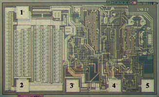
the die is coated with 0.5µm GOLD , which makes it compatible with AuSi or AuGe die attach. L4812 DIE LAYOUT - MECHANICAL SPECIFICATIONS
L4812 DIE LAYOUT - MECHANICAL SPECIFICATIONS PAD # FUNCTION X(mils) X(mm) Y(mils) 1 INPUT 10.827 0.275 50.394 2 OUTPUT 10.827 0.275 3.543 3
OUTPUT 42.52 1.08 3.543 4 GND 69.488 1.765 3.543 5 SHUTDOWN 90.354 2.295 3.543 SEMICONDUCTOR ASSEMBLY PROCESS - SHORT APPLICATION NOTE
Semiconix standard bare die components are designed for thermosonic GOLD wire bonding and AuSi eutectic die attach. For AuSn or AuGe die
attach process, Ti/Pt/Au or Ti/Pd/Au are recommended backside metallization. For soft solder die attach, backside metallization may be any
of Ti/Ni/Au, Ti/Pt/Au, Ti/Pd/Au. For silver filled conductive epoxy die attach, AuSi as well as Ti/Ni/Au, Ti/Pt/Au, Ti/Pd/Au may be used.
In general, after die attach, prior to wire bonding operation an oxygen RF plasma clean operation is recommended. IMPORTANT NOTE: Aluminum
wire should not be used with gold pads due to potential reliability problem known as purple plague. Same it applies to Aluminum bonding
pads with gold wire! In the transition from SnPb solder to lead free and RoHS compliant packaging and assembly processes the reflow
temperature has increased in some cases from 180°C to 220°C. This may cause an increase of the rate of formation of gold aluminum
intermetallic compounds that are brittle and are conducive to increased contact resistance and or bond failure. See Application note
AN-SMX-000. L4812 STANDARD PRODUCTS PRICE LIST USM PART # MINIMUM ORDER QUANTITY Waffle Packs U/P($) USM L4812 100pc -WP $3.20 Products
sold for space, military or medical applications, element evaluation and/or level K or S qualification are subject to minimum order levels
to be established on a case by case basis. For any special applications, die level KGD qualification requirements, different packaging or
custom configurations, contact sales department. /cgi-bin/rfq.cgi" method="post" target="new"> INSTANT QUOTE Semiconix P/N Quantity E-mail
DISCLAIMER - SEMICONIX has made every effort to have this information as accurate as possible. However, no responsibility is assumed by
SEMICONIX for its use, nor for any infringements of rights of third parties, which may result from its use. SEMICONIX reserves the right to
revise the content or modify its product line without prior notice. SEMICONIX products are not authorized for and should not be used within
support systems, which are intended for surgical implants into the body, to support or sustain life, in aircraft, space equipment,
submarine, or nuclear facility applications without the specific written consent. HOME PRODUCT TREE PACKAGES
/cgi-bin/getpdf.pl?part=SMXL4812&idx=4">PDF VERSION SEARCH SEMICONIX SEMICONDUCTOR www.semiconix-semiconductor.com
Tel:(408)986-8026 Fax:(408)986-8027 SEMICONIX SEMICONDUCTOR Last updated: Display settings for best viewing: Current display settings: Page
hits: Screen resolution: 1124x864 Screen resolution: Total site visits: Color quality: 16 bit Color quality: bit © 1990- SEMICONIX
SEMICONDUCTOR All rights reserved. No material from this site may be used or reproduced without permission. Valid XHTML 1.0 Transitional by
http://validator.w3.org
|


