Current regulating diode, current limiting diode, constant current diode: SMSJ511 Current Regulating Diodes same as Linear Integrated Systems J511 Linear Integrated Systems J511 manufactured by Semiconix Semiconductor - Gold chip technology for known good Current regulating diode die, Current regulating diode flip chip, Current regulating diode die, wafer foundry for discrete semiconductors, integrated circuits and integrated passive components from Semiconix Semiconductor Current regulating diode, current limiting diode, constant current diode: SMSJ511 Current Regulating Diodes same as Linear Integrated Systems J511 Linear Integrated Systems J511 manufactured by Semiconix Semiconductor - Gold chip technology for known good Current regulating diode die, Current regulating diode flip chip, Current regulating diode die, wafer foundry for discrete semiconductors, integrated circuits and integrated passive components manufactured by Semiconix Semiconductor. Gold metallization for interconnections instead of aluminum or copper, for high reliability devices for system in package applications using silicon printed circuit boards, ceramic substrates or chip on board, assembled via flip chip or chip and wire. Linear Integrated Systems J511 Linear Integrated Systems J511,SMSJ511,Single,,current regulating diode, current limiting diode, constant current diode, constant-current diode,gold,chip,goldchip,gold chip technology, known good die, flip chip, bare die, wafer foundry, discrete semiconductors, integrated circuits, integrated passive components,gold metallization, aluminum, copper, system in package, SIP, silicon printed circuit board, silicon PCB, ceramic substrates, chip on board, flip chip, chip and gold wire Current regulating diode, current limiting diode, constant current diode: SMSJ511 Current Regulating Diodes same as Linear Integrated Systems J511 Linear Integrated Systems J511 manufactured by Semiconix Semiconductor - Gold chip technology for known good Current regulating diode die, Current regulating diode flip chip, Current regulating diode die, wafer foundry for discrete semiconductors, integrated circuits and integrated passive components from Semiconix Semiconductor Current regulating diode, current limiting diode, constant current diode: SMSJ511 Current Regulating Diodes same as Linear Integrated Systems J511 Linear Integrated Systems J511 manufactured by Semiconix Semiconductor - Gold chip technology for known good Current regulating diode die, Current regulating diode flip chip, Current regulating diode die, wafer foundry for discrete semiconductors, integrated circuits and integrated passive components manufactured by Semiconix Semiconductor. Gold metallization for interconnections instead of aluminum or copper, for high reliability devices for system in package applications using silicon printed circuit boards, ceramic substrates or chip on board, assembled via flip chip or chip and wire. Linear Integrated Systems J511 Linear Integrated Systems J511,SMSJ511,Single,,current regulating diode, current limiting diode, constant current diode, constant-current diode,gold,chip,goldchip,gold chip technology, known good die, flip chip, bare die, wafer foundry, discrete semiconductors, integrated circuits, integrated passive components,gold metallization, aluminum, copper, system in package, SIP, silicon printed circuit board, silicon PCB, ceramic substrates, chip on board, flip chip, chip and gold wire REGISTER-LOGIN PRODUCTS CROSS REFERENCE INVENTORY REQUEST QUOTE ORDER ONLINE SITE MAP semiconix semiconductor - where the future is today - gold chip technology SMSJ511 - BARE DIE GOLD CHIP TECHNOLOGY™ Current Regulating Diodes FEATURES APPLICATIONS CURRENT REGULATING DIODES - BARE DIE Same as Linear Integrated Systems J511 SECOND SOURCE FOR SILICONIX J500 SERIES WIDE CURRENT RANGE 0.43 to 4.7mA BIASING NOT REQUIRED VGS=0V Available in bare die form, flip chip, µDFN, SOT-23 and TO92 Ideal for Current Limiting and Constant Current Applications High reliability bare die Gold metallization RoHS compliant, Lead Free Compatible with chip and wire assemblies Current limiting Constant current applications Chip on Board System in package SIP Hybrid Circuits SMSJ511 J511 Current Regulating Diodes Current Regulating Diodes - PRODUCT DESCRIPTION Current regulating diode (also called CLD, current limiting diode, Constant current diode, constant-current diode, diode-connected transistor or current-regulating diode) is actually a JFET with the gate shorted to the source, and it functions like a two-terminal current limiter or current source (analog to voltage limiting Zener diode). They allow a current through them to rise to a certain value, and then level off at a specific value. Current Regulating Diodes BD series are available in die form in two configurations, Top Cathode XXXX-BD or Top Anode XXXXA-BD. In die form, these products are ideal for high reliability hybrid circuits and multi chip module applications. HIGH RELIABILITY BARE DIE AND SYSTEM IN PACKAGE - SHORT APPLICATION NOTE COB (Chip on Board) and SiP (System-in-Package) are integrating proven mature products in bare die of mixed technologies i.e. Si, GaAs, GaN, InP, passive components, etc that cannot be easily implemented in SOC (System-on-Chip) technology. COB and SiP have small size footprint, high density, shorter design cycle time, easier to redesign and rework, use simpler and less expensive assembly process. For extreme applications the bare die has to withstand also harsh environmental conditions without the protection of a package. KGD, Known Good Die concept is no longer satisfactory if the die cannot withstand harsh environmental conditions and degrades. Standard semiconductor devices supplied by many manufacturers in bare die are build with exposed aluminum pads that are extremely sensitive to moisture and corrosive components of the atmosphere. Semiconix has reengineered industry standard products and now offers known good die for bare die applications with gold interconnection and well-engineered materials that further enhance the die reliability. Semiconix also offers Silicon Printed Circuit Board technology with integrated passive components as a complete high reliability SIP solution for medical, military and space applications. See AN-SMX-001 DISCRETE SEMICONDUCTORS MANUFACTURING PROCESS Discrete semiconductors are manufactured using Semiconix in house high reliability semiconductor manufacturing processes. All semiconductor devices employ precision doping via ion implantation, silicon nitride junction passivation, platinum silicided contacts and gold interconnect metallization for best performance and reliability. MNOS capacitors, Tantalum Nitride TaN or Sichrome SiCr thin film resistors are easily integrated with discrete semiconductors on same chip to obtain standard and custom complex discrete device solutions. ABSOLUTE MAXIMUM RATINGS @ 25 °C (unless otherwise stated) Parameter Symbol Value Unit Maximum Storage Temperature TSTG -55 to +150 °C Maximum Operating Junction Temperature TJ -55 to +135 °C Maximum Continuous Power Dissipation @ +125 °C PD 360 mW Forward Current IF 20 mA Reverse Current IR 50 mA Peak Operating Voltage POV 50 V Electrical Characteristics* TC = 25°C unless otherwise noted Name Symbol Test Conditions Value Unit Min. Typ. Max Forward Current IF VF= 25V 3.8 4.7 5.6 mA Dynamic Impedance Zd VF= 25V 0.12 0.3 Ω Knee Impedance Zk VF= 6V 0.05 Ω Limiting Voltage Vl IF= 0.8IF(min) 4.2 2.1 V Peak Operating Voltage Pov IF= 1.1IF(max) 50 V Reverse Voltage VF IR=1mA 0.8 V Forward Capacitance CF VF= 25V, f= 1MHz 2.2 pF Absolute maximum ratings are limiting values above which serviceability may be impaired. Pulsed, t = 2ms. Maximum VF where IF < 1.1IF(max). Pulsed, t = 2ms. Continuous currents may vary. Pulsed, t = 2ms. Continuous impedances may vary. Min VF required to ensure IF = 0.8IF(min). SPICE MODEL Spice model pending. CROSS REFERENCE PARTS: Linear Integrated Systems J511 GENERAL DIE INFORMATION Substrate Thickness [mils] Die size [mils] Bonding pads Backside metallization Silicon 6±1 20x10±2 Pad metal is TiW/Au, 4µm±1 thick, 99.99% electroplated gold with TiW barrier. Custom metallization available upon request. P/N Metal Die attach process -BD0 Au/Si Au/Si eutectic -BD1 Ti/Pd/Au AuSn,AuGe -BD2 Ti/Pt/Au AuSn,AuGe -BD3 Ti/Ni/Au Soft Solder SAC -BD4 Ti/Pt/AuSn AuSn eutectic LAYOUT / DIMENSIONS / PAD LOCATIONS Click to select → TOP CATHODE TOP ANODE TOP CATHODE SMSJ511 Linear Integrated Systems J511 Linear Integrated Systems J511 Current Regulating DiodesTOP ANODE SMSJ511 Linear Integrated Systems J511 Linear Integrated Systems J511 Current Regulating Diodes cathode SMSJ511 Linear Integrated Systems J511 Linear Integrated Systems J511 Current Regulating Diodesanode SMSJ511 Linear Integrated Systems J511 Linear Integrated Systems J511 Current Regulating Diodes SMSJ511 Linear Integrated Systems J511 Linear Integrated Systems J511 Current Regulating Diodes SEMICONDUCTOR ASSEMBLY PROCESS - SHORT APPLICATION NOTE Semiconix standard bare die components are designed for thermosonic GOLD wire bonding and AuSi eutectic die attach. For AuSn or AuGe die attach process, Ti/Pt/Au or Ti/Pd/Au are recommended backside metallization. For soft solder die attach, backside metallization may be any of Ti/Ni/Au, Ti/Pt/Au, Ti/Pd/Au. For silver filled conductive epoxy die attach, AuSi as well as Ti/Ni/Au, Ti/Pt/Au, Ti/Pd/Au may be used. In general, after die attach, prior to wire bonding operation an oxygen RF plasma clean operation is recommended. IMPORTANT NOTE: Aluminum wire should not be used with gold pads due to potential reliability problem known as purple plague. Same it applies to Aluminum bonding pads with gold wire! In the transition from SnPb solder to lead free and RoHS compliant packaging and assembly processes the reflow temperature has increased in some cases from 180°C to 220°C. This may cause an increase of the rate of formation of gold aluminum intermetallic compounds that are brittle and are conducive to increased contact resistance and or bond failure. See Application note AN-SMX-000. STANDARD PRODUCTS ORDERING INFORMATION SMS P/N WAFFLE PACKS QUANTITY U/P($) FILM FRAME MIN QUANTITY U/P($) SMSJ511-BD -WP 10000 -FF 45000 SMSJ511-BD -WP 50000 -FF 225000 SMSJ511A-BD -WP 10000 -FF 45000 SMSJ511A-BD -WP 50000 -FF 225000 PRICES - Listed prices are only for standard products, available from stock. Inventory is periodically updated. List prices for other quantities and tolerances are available on line through Instant Quote. For standard products available from stock, there is a minimum line item order of $550.00. No rights can be derived from pricing information provided on this website. Such information is indicative only, for budgetary use only and subject to change by SEMICONIX SEMICONDUCTOR at any time and without notice. LEAD TIMES - Typical delivery for standard products is 4-6 weeks ARO. For custom devices consult factory for an update on minim orders and lead times. CONTINOUS SUPPLY - Semiconix guarantees continuous supply and availability of any of its standard products provided minimum order quantities are met. CUSTOM PRODUCTS - For custom products sold as tested, bare die or known good die KGD, there will be a minimum order quantity MOQ. Dice are 100% functional tested, visual inspected and shipped in antistatic waffle packs. For high volume and pick and place applications, dice are also shipped on film frame -FF. For special die level KGD requirements, different packaging or custom configurations, contact sales via CONTACTS page. SAMPLES - Samples are available only for customers that have issued firm orders pending qualification of product in a particular application. ORDERING - Semiconix accepts only orders placed on line by registered customers. On line orders are verified, accepted and acknowledged by Semiconix sales department in writing. Accepted orders are non cancelable binding contracts. SHIPING - Dice are 100% functional tested, visual inspected and shipped in antistatic waffle packs. For high volume and pick and place applications, dice are also shipped on film frame -FF. INSTANT QUOTE Semiconix P/N Quantity E-mail DISCLAIMER - SEMICONIX has made every effort to have this information as accurate as possible. However, no responsibility is assumed by SEMICONIX for its use, nor for any infringements of rights of third parties, which may result from its use. SEMICONIX reserves the right to revise the content or modify its product line without prior notice. SEMICONIX products are not authorized for and should not be used within support systems, which are intended for surgical implants into the body, to support or sustain life, in aircraft, space equipment, submarine, or nuclear facility applications without the specific written consent. HOME PRODUCT TREE PACKAGES PDF VERSION SEARCH SEMICONIX SEMICONDUCTOR www.semiconix-semiconductor.com Tel:(408)986-8026 Fax:(408)986-8027 SEMICONIX SEMICONDUCTOR Last updated:January 01, 1970 Display settings for best viewing: Current display settings: Page hits: 17 Screen resolution: 1124x864 Screen resolution: Total site visits: 326577 Color quality: 16 bit Color quality: bit © 1990-2009 SEMICONIX SEMICONDUCTOR All rights reserved. No material from this site may be used or reproduced without permission.

REGISTER-LOGIN PRODUCTS CROSS REFERENCE INVENTORY REQUEST QUOTE ORDER ONLINE SITE MAP

   
semiconix semiconductor - where the future is today - gold chip technology SMSJ511 - BARE DIE
GOLD CHIP TECHNOLOGY™ Current Regulating Diodes

FEATURES APPLICATIONS CURRENT REGULATING DIODES - BARE DIE
Same as Linear Integrated Systems J511
SECOND SOURCE FOR SILICONIX J500 SERIES
WIDE CURRENT RANGE 0.43 to 4.7mA
BIASING NOT REQUIRED VGS=0V
Available in bare die form, flip chip, µDFN, SOT-23 and TO92
Ideal for Current Limiting and Constant Current Applications
High reliability bare die
Gold metallization
RoHS compliant, Lead Free
Compatible with chip and wire assemblies
Current limiting
Constant current applications
Chip on Board
System in package SIP
Hybrid Circuits
SMSJ511 J511 Current Regulating Diodes

Current Regulating Diodes - PRODUCT DESCRIPTION
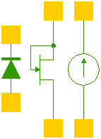
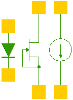
Current regulating diode (also called CLD, current limiting diode, Constant current diode, constant-current diode, diode-connected transistor or current-regulating diode) is actually a JFET with the gate shorted to the source, and it functions like a two-terminal current limiter or current source (analog to voltage limiting Zener diode). They allow a current through them to rise to a certain value, and then level off at a specific value.
Current Regulating Diodes BD series are available in die form in two configurations, Top Cathode XXXX-BD or Top Anode XXXXA-BD. In die form, these products are ideal for high reliability hybrid circuits and multi chip module applications.

HIGH RELIABILITY BARE DIE AND SYSTEM IN PACKAGE - SHORT APPLICATION NOTE
COB (Chip on Board) and SiP (System-in-Package) are integrating proven mature products in bare die of mixed technologies i.e. Si, GaAs, GaN, InP, passive components, etc that cannot be easily implemented in SOC (System-on-Chip) technology. COB and SiP have small size footprint, high density, shorter design cycle time, easier to redesign and rework, use simpler and less expensive assembly process. For extreme applications the bare die has to withstand also harsh environmental conditions without the protection of a package. KGD, Known Good Die concept is no longer satisfactory if the die cannot withstand harsh environmental conditions and degrades. Standard semiconductor devices supplied by many manufacturers in bare die are build with exposed aluminum pads that are extremely sensitive to moisture and corrosive components of the atmosphere. Semiconix has reengineered industry standard products and now offers known good die for bare die applications with gold interconnection and well-engineered materials that further enhance the die reliability. Semiconix also offers Silicon Printed Circuit Board technology with integrated passive components as a complete high reliability SIP solution for medical, military and space applications. See AN-SMX-001

DISCRETE SEMICONDUCTORS MANUFACTURING PROCESS
Discrete semiconductors are manufactured using Semiconix in house high reliability semiconductor manufacturing processes. All semiconductor devices employ precision doping via ion implantation, silicon nitride junction passivation, platinum silicided contacts and gold interconnect metallization for best performance and reliability. MNOS capacitors, Tantalum Nitride TaN or Sichrome SiCr thin film resistors are easily integrated with discrete semiconductors on same chip to obtain standard and custom complex discrete device solutions.

ABSOLUTE MAXIMUM RATINGS @ 25 °C (unless otherwise stated)
Parameter Symbol Value Unit
Maximum Storage Temperature TSTG -55 to +150 °C
Maximum Operating Junction Temperature TJ -55 to +135 °C
Maximum Continuous Power Dissipation @ +125 °C PD 360 mW
Forward Current IF 20 mA
Reverse Current IR 50 mA
Peak Operating Voltage POV 50 V

Electrical Characteristics* TC = 25°C unless otherwise noted
Name Symbol Test Conditions Value Unit
Min. Typ. Max
Forward Current IF VF= 25V 3.8 4.7 5.6 mA
Dynamic Impedance Zd VF= 25V 0.12 0.3 Ω
Knee Impedance Zk VF= 6V 0.05 Ω
Limiting Voltage Vl IF= 0.8IF(min) 4.2 2.1 V
Peak Operating Voltage Pov IF= 1.1IF(max) 50 V
Reverse Voltage VF IR=1mA 0.8 V
Forward Capacitance CF VF= 25V, f= 1MHz 2.2 pF
Absolute maximum ratings are limiting values above which serviceability may be impaired.
Pulsed, t = 2ms. Maximum VF where IF < 1.1IF(max).
Pulsed, t = 2ms. Continuous currents may vary.
Pulsed, t = 2ms. Continuous impedances may vary.
Min VF required to ensure IF = 0.8IF(min).
SPICE MODEL
Spice model pending.
CROSS REFERENCE PARTS: Linear Integrated Systems J511

GENERAL DIE INFORMATION
Substrate Thickness
[mils]
Die size
[mils]
Bonding pads Backside metallization
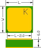
Silicon 6±1 20x10±2 Pad metal is TiW/Au, 4µm±1 thick, 99.99% electroplated gold with TiW barrier. Custom metallization available upon request.
P/N MetalDie attach process
-BD0Au/SiAu/Si eutectic
-BD1Ti/Pd/AuAuSn,AuGe
-BD2Ti/Pt/AuAuSn,AuGe
-BD3Ti/Ni/AuSoft Solder SAC
-BD4Ti/Pt/AuSnAuSn eutectic

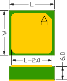
LAYOUT / DIMENSIONS / PAD LOCATIONS
Click to select → TOP CATHODE TOP ANODE
TOP CATHODE SMSJ511 Linear Integrated Systems J511 Linear Integrated Systems J511 Current Regulating Diodes
cathode SMSJ511 Linear Integrated Systems J511 Linear Integrated Systems J511 Current Regulating Diodes
SMSJ511 Linear Integrated Systems J511 Linear Integrated Systems J511 Current Regulating Diodes

SEMICONDUCTOR ASSEMBLY PROCESS - SHORT APPLICATION NOTE
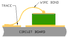
Semiconix standard bare die components are designed for thermosonic GOLD wire bonding and AuSi eutectic die attach. For AuSn or AuGe die attach process, Ti/Pt/Au or Ti/Pd/Au are recommended backside metallization.
For soft solder die attach, backside metallization may be any of Ti/Ni/Au, Ti/Pt/Au, Ti/Pd/Au.
For silver filled conductive epoxy die attach, AuSi as well as Ti/Ni/Au, Ti/Pt/Au, Ti/Pd/Au may be used.
In general, after die attach, prior to wire bonding operation an oxygen RF plasma clean operation is recommended.
IMPORTANT NOTE: Aluminum wire should not be used with gold pads due to potential reliability problem known as purple plague. Same it applies to Aluminum bonding pads with gold wire! In the transition from SnPb solder to lead free and RoHS compliant packaging and assembly processes the reflow temperature has increased in some cases from 180°C to 220°C. This may cause an increase of the rate of formation of gold aluminum intermetallic compounds that are brittle and are conducive to increased contact resistance and or bond failure. See Application note AN-SMX-000.

STANDARD PRODUCTS ORDERING INFORMATION

SMS P/N WAFFLE PACKS QUANTITY U/P($) FILM FRAME MIN QUANTITY U/P($)
SMSJ511-BD -WP 10000 -FF 45000
SMSJ511-BD -WP 50000 -FF 225000
SMSJ511A-BD -WP 10000 -FF 45000
SMSJ511A-BD -WP 50000 -FF 225000

PRICES - Listed prices are only for standard products, available from stock. Inventory is periodically updated. List prices for other quantities and tolerances are available on line through Instant Quote. For standard products available from stock, there is a minimum line item order of $550.00. No rights can be derived from pricing information provided on this website. Such information is indicative only, for budgetary use only and subject to change by SEMICONIX SEMICONDUCTOR at any time and without notice.
LEAD TIMES - Typical delivery for standard products is 4-6 weeks ARO. For custom devices consult factory for an update on minim orders and lead times.
CONTINOUS SUPPLY - Semiconix guarantees continuous supply and availability of any of its standard products provided minimum order quantities are met.
CUSTOM PRODUCTS - For custom products sold as tested, bare die or known good die KGD, there will be a minimum order quantity MOQ. Dice are 100% functional tested, visual inspected and shipped in antistatic waffle packs. For high volume and pick and place applications, dice are also shipped on film frame -FF. For special die level KGD requirements, different packaging or custom configurations, contact sales via CONTACTS page.
SAMPLES - Samples are available only for customers that have issued firm orders pending qualification of product in a particular application.
ORDERING - Semiconix accepts only orders placed on line by registered customers. On line orders are verified, accepted and acknowledged by Semiconix sales department in writing. Accepted orders are non cancelable binding contracts.
SHIPING - Dice are 100% functional tested, visual inspected and shipped in antistatic waffle packs. For high volume and pick and place applications, dice are also shipped on film frame -FF.

INSTANT QUOTE
Semiconix P/N Quantity E-mail    

DISCLAIMER - SEMICONIX has made every effort to have this information as accurate as possible. However, no responsibility is assumed by SEMICONIX for its use, nor for any infringements of rights of third parties, which may result from its use. SEMICONIX reserves the right to revise the content or modify its product line without prior notice. SEMICONIX products are not authorized for and should not be used within support systems, which are intended for surgical implants into the body, to support or sustain life, in aircraft, space equipment, submarine, or nuclear facility applications without the specific written consent.

HOME PRODUCT TREE PACKAGES PDF VERSION SEARCH

SEMICONIX SEMICONDUCTOR www.semiconix-semiconductor.com
Tel:(408)758-8694 Fax:(408)986-8027
SEMICONIX SEMICONDUCTOR
Last updated:July 06, 2009 Display settings for best viewing: Current display settings:
Page hits: 1112 Screen resolution: 1124x864 Screen resolution:
Total site visits: 20804607 Color quality: 16 bit Color quality: bit
© 1990-2024 SEMICONIX SEMICONDUCTOR All rights reserved. No material from this site may be used or reproduced without permission.