|
SMX LM339 QUAD SINGLE SUPPLY COMPARATORS same as Texas Instruments LM339, manufactured by Semiconix Semiconductor - Gold chip technology for known good die, flip chip, bare die, wafer foundry for discrete semiconductors, integrated circuits and integrated passive components from Semiconix Semiconductor - Goldchip technology is trademark of Semiconix Corporation for known good die, flip chip, bare die, wafer foundry for discrete semiconductors, integrated circuits and integrated passive components manufactured by Semiconix Semiconductor. Gold metallization for interconnections instead of aluminum or copper, for high reliability devices for system in package applications using silicon printed circuit boards, ceramic substrates or chip on board, assembled via flip chip or chip and wire.
SMX LM339 QUAD SINGLE SUPPLY COMPARATORS same as Texas Instruments LM339, manufactured by Semiconix Semiconductor - Gold chip
technology for known good die, flip chip, bare die, wafer foundry for discrete semiconductors, integrated circuits and integrated passive
components from Semiconix Semiconductor - Goldchip technology is trademark of Semiconix Corporation for known good die, flip chip, bare
die, wafer foundry for discrete semiconductors, integrated circuits and integrated passive components manufactured by Semiconix
Semiconductor. Gold metallization for interconnections instead of aluminum or copper, for high reliability devices for system in package
applications using silicon printed circuit boards, ceramic substrates or chip on board, assembled via flip chip or chip and wire.
REGISTER-LOGIN PRODUCTS CROSS REFERENCE /cgi-bin/stock.pl?part=LM339">INVENTORY
/cgi-bin/rfq.cgi?site=4&rows=1&item_1=SMXLM339&c_item_1=">REQUEST QUOTE smxrootwww.semiconix.com/cgi-bin/order.cgi?site=">ORDER ONLINE SITE
MAP semiconix semiconductor - where the future is today - gold chip technology SMX LM339 - BARE DIE GOLD CHIP TECHNOLOGY™ QUAD SINGLE
SUPPLY COMPARATORS FEATURES APPLICATIONS QUAD SINGLE SUPPLY COMPARATORS Wide single supply 2.0V to 36V Dual supplies:±1.0V to ±18V Very low
supply current drain (0.4 mA) independent of supply voltage In DIE form, this device is an excellent selection for many chip and wire
HYBRID CIRCUITS LM339 LM339 QUAD SINGLE SUPPLY COMPARATORS SMXLM339 QUAD SINGLE SUPPLY COMPARATORS - PRODUCT DESCRIPTION The SMX LM339
series are dual independent precision voltage comparators capable of single or split power supply operation. These devices are designed to
permit a common mode rangetoground level with single supply operation. HIGH RELIABILITY BARE DIE AND SYSTEM IN PACKAGE - SHORT
APPLICATION NOTE COB (Chip on Board) and SiP (System-in-Package) are integrating proven mature products in bare die of mixed technologies
i.e. Si, GaAs, GaN, InP, passive components, etc that cannot be easily implemented in SOC (System-on-Chip) technology. COB and SiP have
small size footprint, high density, shorter design cycle time, easier to redesign and rework, use simpler and less expensive assembly
process. For extreme applications the bare die has to withstand also harsh environmental conditions without the protection of a package.
KGD, Known Good Die concept is no longer satisfactory if the die cannot withstand harsh environmental conditions and degrades. Standard
semiconductor devices supplied by many manufacturers in bare die are build with exposed aluminum pads that are extremely sensitive to
moisture and corrosive components of the atmosphere. Semiconix has reengineered industry standard products and now offers known good die
for bare die applications with gold interconnection and well-engineered materials that further enhance the die reliability. Semiconix also
offers Silicon Printed Circuit Board technology with integrated passive components as a complete high reliability SIP solution for medical,
military and space applications. See AN-SMX-001 SEMICONDUCTOR INTEGRATED CIRCUITS MANUFACTURING PROCESS Semiconductor Integrated Circuits
are manufactured using Semiconix in house high reliability semiconductor manufacturing processes. All semiconductor devices employ
precision doping via ion implantation, silicon nitride junction passivation, platinum silicided contacts and gold interconnect
metallization for best performance and reliability. MNOS capacitors, Tantalum Nitride TaN or Sichrome SiCr thin film resistors are easily
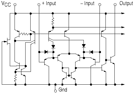
integrated with other semiconductor devices on same chip to obtain standard and custom complex device solutions. SCHEMATIC DIAGRAM LM339
Texas Instruments LM339 QUAD SINGLE SUPPLY COMPARATORS LM339 MAXIMUM RATINGS PARAMETER SYMBOL VALUE UNITS Power Supply Voltages Vcc +36 or
18 Vdc Input Differential Voltage Range Vdir 32 Vdc Input Common Mode Voltage Range Vicmr -0.3 to VCC Vdc Output Short Circuit to Ground
Isc Continuous Power dissipation TA = 25°C Derate Above 25°C PD 8 mW/°C Junction temperature Tj 150 °C Operating Ambient Temperature Range
Topa 0 to +70 °C Storage Temperature Range Tstg -65 to +150 °C ONLY Proper die handling equipment and procedures should be employed.
Stresses beyond listed absolute maximum ratings may cause permanent damage to the device. LM339 ELECTRICAL CHARACTERISTIC VCC = +5.0 Vdc,
TA = +25°C, unless otherwise specified PARAMETER TEST CONDITIONS SYMBOL MIN TYP MAX UNITS Input Offset Voltage (Note1) VIO ±2.0 ±5.0 mVdc
Input Bias Current (Note1, Note 2) IIB 25 250 nA Input Offset Current (Note 1) IIO ±5.0 ±5.0 nA Input Common Mode Voltage Range VICMR
VCC-1.5 V Supply Current RL=¥, RL=¥, VCC = 30 Vdc ICC - - 0.8 1.0 2.0 2.5 mA Voltage Gain RL ≥15 k, VCC = 15 Vdc AVOL 50 200 V/mV Large
Signal Response Time VI = TTL Logic Swing, Vref = 1.4 Vdc, VRL = 5.0 Vdc, RL = 5.1 kW - 300 ns Response Time (Note 6) VRL = 5.0 Vdc, RL =
5.1 kW - 1.3 µs Output Sink Current VI (-)≥+1.0 Vdc, VI(+) = 0,VO≤1.5 Vdc ISINK 6 16 mA Saturation Voltage VI(-)≥+1.0 Vdc, VI(+) = 0,
Isink≤4.0 mA Vsat 130 400 mV Output Leakage Current VI(+)≥+1.0 Vdc, VI(-) = 0, VO = +5.0 Vdc IOL 0.1 nA (NOTE 1)At the output switch point,
V O 1.4 Vdc, RS £ 100 5.0 Vdc £ VCC £ 30 Vdc, with the inputs over the full common mode range (0 Vdc to VCC 1.5 Vdc). (NOTE 2)The bias
current flows out of the inputs due to the PNP input stage. This current is virtually constant, independent of the output state. SPICE
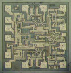
MODEL CROSS REFERENCE PARTS GENERAL DIE INFORMATION Substrate Thickness [mils] Die size mils [mm] Bonding pads Backside metallization
Silicon 10 61.024 x 62.992 ±1 [1.55 x 1.6] 4.724x4.724 Backside of the die is coated with 0.5µm GOLD , which makes it compatible with AuSi
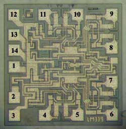
or AuGe die attach. LM339 DIE LAYOUT - MECHANICAL SPECIFICATIONS LM339 DIE LAYOUT - MECHANICAL SPECIFICATIONS PAD # FUNCTION X(mils) X(mm)
Y(mils) 1 OUT#1 0.105 4.134 0.718 2 OUT#2 0.105 4.134 0.333 3 VCC 0.105 4.134 0.11 4 IN-#2 0.48 18.898 0.11 5 IN+#2 0.99 38.976 0.11 6
IN-#1 1.325 52.165 0.11 7 IN+#1 1.325 52.165 0.53 8 IN-#3 1.325 52.165 0.949 9 IN+#3 1.325 52.165 1.369 10 IN-#4 0.99 38.976 1.369 11 IN+#4
0.48 18.898 1.369 12 GND 0.105 4.134 1.369 13 OUT#4 0.105 4.134 1.118 14 OUT#3 0.105 4.134 0.928 SEMICONDUCTOR ASSEMBLY PROCESS - SHORT
APPLICATION NOTE Semiconix standard bare die components are designed for thermosonic GOLD wire bonding and AuSi eutectic die attach. For
AuSn or AuGe die attach process, Ti/Pt/Au or Ti/Pd/Au are recommended backside metallization. For soft solder die attach, backside
metallization may be any of Ti/Ni/Au, Ti/Pt/Au, Ti/Pd/Au. For silver filled conductive epoxy die attach, AuSi as well as Ti/Ni/Au,
Ti/Pt/Au, Ti/Pd/Au may be used. In general, after die attach, prior to wire bonding operation an oxygen RF plasma clean operation is
recommended. IMPORTANT NOTE: Aluminum wire should not be used with gold pads due to potential reliability problem known as purple plague.
Same it applies to Aluminum bonding pads with gold wire! In the transition from SnPb solder to lead free and RoHS compliant packaging and
assembly processes the reflow temperature has increased in some cases from 180°C to 220°C. This may cause an increase of the rate of
formation of gold aluminum intermetallic compounds that are brittle and are conducive to increased contact resistance and or bond failure.
See Application note AN-SMX-000. LM339 STANDARD PRODUCTS PRICE LIST USM PART # MINIMUM ORDER QUANTITY Waffle Packs U/P($) USMLM339 100pc
-WP $3.20 Products sold for space, military or medical applications, element evaluation and/or level K or S qualification are subject to
minimum order levels to be established on a case by case basis. For any special applications, die level KGD qualification requirements,
different packaging or custom configurations, contact sales department. /cgi-bin/rfq.cgi" method="post" target="new"> INSTANT QUOTE
Semiconix P/N Quantity E-mail DISCLAIMER - SEMICONIX has made every effort to have this information as accurate as possible. However, no
responsibility is assumed by SEMICONIX for its use, nor for any infringements of rights of third parties, which may result from its use.
SEMICONIX reserves the right to revise the content or modify its product line without prior notice. SEMICONIX products are not authorized
for and should not be used within support systems, which are intended for surgical implants into the body, to support or sustain life, in
aircraft, space equipment, submarine, or nuclear facility applications without the specific written consent. HOME PRODUCT TREE PACKAGES
/cgi-bin/getpdf.pl?part=SMXLM339&idx=8">PDF VERSION SEARCH SEMICONIX SEMICONDUCTOR www.semiconix-semiconductor.com
Tel:(408)986-8026 Fax:(408)986-8027 SEMICONIX SEMICONDUCTOR Last updated: Display settings for best viewing: Current display settings: Page
hits: Screen resolution: 1124x864 Screen resolution: Total site visits: Color quality: 16 bit Color quality: bit © 1990- SEMICONIX
SEMICONDUCTOR All rights reserved. No material from this site may be used or reproduced without permission. Valid XHTML 1.0 Transitional by
http://validator.w3.org
|


