|
SMX LM555 TIMER same as National Semiconductor LM555, Fairchild Semiconductor LM555, Fairchild Semiconductor LM555CN, Fairchild Semiconductor LM555CM, Fairchild Semiconductor LM555CMX, Harris Semiconductor LM555N, Harris Semiconductor LM555N, Intersil LM555CN, Intersil LM555C, National Semiconductor LM555H-MLS, National Semiconductor LM555CMX, National Semiconductor LM555CMX, National Semiconductor LM555CMX, National Semiconductor LM555H/883, National Semiconductor LM555J/883, National Semiconductor LM555CN, National Semiconductor LM555CN, National Semiconductor LM555CN, National Semiconductor LM555H-MLS, National Semiconductor LM555H-MLS, National Semiconductor LM555J/883, National Semiconductor LM555H/883, National Semiconductor LM555H/883, National Semiconductor LM555J/883, National Semiconductor LM555CMMX, National Semiconductor LM555 MWC, National Semiconductor LM555 MWC, National Semiconductor LM555 MDC, National Semiconductor LM555 MDC, National Semiconductor LM555 MDC, National Semiconductor LM555 MD8, National Semiconductor LM555 MD8, National Semiconductor LM555 MD8, National Semiconductor LM555 MWC, National Semiconductor LM555C, National Semiconductor LM555CMMX, National Semiconductor LM555CMMX, National Semiconductor LM555CMM, National Semiconductor LM555CMM, National Semiconductor LM555CMM, National Semiconductor LM555CM, National Semiconductor LM555CM, National Semiconductor LM555CM, National Semiconductor LM555 manufactured by Semiconix Semiconductor - Gold chip technology for known good die, flip chip, bare die, wafer foundry for discrete semiconductors, integrated circuits and integrated passive components from Semiconix Semiconductor - Goldchip technology is trademark of Semiconix Corporation for known good die, flip chip, bare die, wafer foundry for discrete semiconductors, integrated circuits and integrated passive components manufactured by Semiconix Semiconductor. Gold metallization for interconnections instead of aluminum or copper, for high reliability devices for system in package applications using silicon printed circuit boards, ceramic substrates or chip on board, assembled via flip chip or chip and wire.
Fairchild Semiconductor LM555, Harris Semiconductor LM555N, Intersil LM555C, National Semiconductor LM555
SMX LM555 TIMER same as National Semiconductor LM555, Fairchild Semiconductor LM555, Fairchild Semiconductor LM555CN, Fairchild
Semiconductor LM555CM, Fairchild Semiconductor LM555CMX, Harris Semiconductor LM555N, Harris Semiconductor LM555N, Intersil LM555CN,
Intersil LM555C, National Semiconductor LM555H-MLS, National Semiconductor LM555CMX, National Semiconductor LM555CMX, National
Semiconductor LM555CMX, National Semiconductor LM555H/883, National Semiconductor LM555J/883, National Semiconductor LM555CN, National
Semiconductor LM555CN, National Semiconductor LM555CN, National Semiconductor LM555H-MLS, National Semiconductor LM555H-MLS, National
Semiconductor LM555J/883, National Semiconductor LM555H/883, National Semiconductor LM555H/883, National Semiconductor LM555J/883, National
Semiconductor LM555CMMX, National Semiconductor LM555 MWC, National Semiconductor LM555 MWC, National Semiconductor LM555 MDC, National
Semiconductor LM555 MDC, National Semiconductor LM555 MDC, National Semiconductor LM555 MD8, National Semiconductor LM555 MD8, National
Semiconductor LM555 MD8, National Semiconductor LM555 MWC, National Semiconductor LM555C, National Semiconductor LM555CMMX, National
Semiconductor LM555CMMX, National Semiconductor LM555CMM, National Semiconductor LM555CMM, National Semiconductor LM555CMM, National
Semiconductor LM555CM, National Semiconductor LM555CM, National Semiconductor LM555CM, National Semiconductor LM555 manufactured by
Semiconix Semiconductor - Gold chip technology for known good die, flip chip, bare die, wafer foundry for discrete semiconductors,
integrated circuits and integrated passive components from Semiconix Semiconductor - Goldchip technology is trademark of Semiconix
Corporation for known good die, flip chip, bare die, wafer foundry for discrete semiconductors, integrated circuits and integrated passive
components manufactured by Semiconix Semiconductor. Gold metallization for interconnections instead of aluminum or copper, for high
reliability devices for system in package applications using silicon printed circuit boards, ceramic substrates or chip on board, assembled
via flip chip or chip and wire. Fairchild Semiconductor LM555, Harris Semiconductor LM555N, Intersil LM555C, National Semiconductor LM555
REGISTER-LOGIN PRODUCTS CROSS REFERENCE /cgi-bin/stock.pl?part=LM555">INVENTORY
/cgi-bin/rfq.cgi?site=4&rows=1&item_1=SMXLM555&c_item_1=">REQUEST QUOTE smxrootwww.semiconix.com/cgi-bin/order.cgi?site=">ORDER ONLINE SITE
MAP semiconix semiconductor - where the future is today - gold chip technology SMX LM555 - BARE DIE GOLD CHIP TECHNOLOGY™ TIMER FEATURES
APPLICATIONS TIMER Direct replacement for SE555/NE555 Timing from micro-seconds through hours Operates in both astable and mono- stable
modes Adjustable duty cycle Output can source or sink 200mA Output and supply TTL compatible Temperature stability better than 0.005% per C
Normally on and normally off output In DIE form, this device is an excellent selection for many chip and wire HYBRID CIRCUITS LM555 LM555
TIMER SMXLM555 TIMER - PRODUCT DESCRIPTION The SMX LM555 is a highly stable device for generating accurate time delays or oscillation.
Additional terminals are provided for triggering or resettin desired. In the time delay mode of operation, the time is precisely controlled
by one external resistor and capacitor. For a stable operation as an oscillator, the free running frequency and duty cycle are accurately
controlled with two external resistors and one capacitor.The circuit may retriggered and reset on falling waveforms, and the output circuit
can source or sink up to 200mA or drive TTL circuits. HIGH RELIABILITY BARE DIE AND SYSTEM IN PACKAGE - SHORT APPLICATION NOTE COB (Chip on
Board) and SiP (System-in-Package) are integrating proven mature products in bare die of mixed technologies i.e. Si, GaAs, GaN, InP,
passive components, etc that cannot be easily implemented in SOC (System-on-Chip) technology. COB and SiP have small size footprint, high
density, shorter design cycle time, easier to redesign and rework, use simpler and less expensive assembly process. For extreme
applications the bare die has to withstand also harsh environmental conditions without the protection of a package. KGD, Known Good Die
concept is no longer satisfactory if the die cannot withstand harsh environmental conditions and degrades. Standard semiconductor devices
supplied by many manufacturers in bare die are build with exposed aluminum pads that are extremely sensitive to moisture and corrosive
components of the atmosphere. Semiconix has reengineered industry standard products and now offers known good die for bare die applications
with gold interconnection and well-engineered materials that further enhance the die reliability. Semiconix also offers Silicon Printed
Circuit Board technology with integrated passive components as a complete high reliability SIP solution for medical, military and space
applications. See AN-SMX-001 SEMICONDUCTOR INTEGRATED CIRCUITS MANUFACTURING PROCESS Semiconductor Integrated Circuits are manufactured
using Semiconix in house high reliability semiconductor manufacturing processes. All semiconductor devices employ precision doping via ion
implantation, silicon nitride junction passivation, platinum silicided contacts and gold interconnect metallization for best performance
and reliability. MNOS capacitors, Tantalum Nitride TaN or Sichrome SiCr thin film resistors are easily integrated with other semiconductor
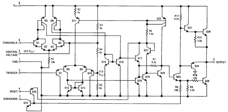
devices on same chip to obtain standard and custom complex device solutions. SCHEMATIC DIAGRAM LM555 National Semiconductor LM555 TIMER
LM555 MAXIMUM RATINGS PARAMETER SYMBOL VALUE UNITS Supply Voltages Vcc 18 V Power Disipation(Note3) LM555CM, LM555CN LM555CMM Pd 1180 603
mW Operating Temperature Ranges LM555C Top 0 to +70 °C Storage Temperature Range Tstg -65 to +150 °C ONLY Proper die handling equipment and
procedures should be employed. Stresses beyond listed absolute maximum ratings may cause permanent damage to the device. LM555 ELECTRICAL
CHARACTERISTIC (Note 1,2 TA=25°C,VCC=+5V to+15V unless otherwise specificed) PARAMETER TEST CONDITIONS SYMBOL MIN TYP MAX UNITS Supply
Voltage 4.5 16 V Supply Curent VCC=5V R=¥ VCC=5V RL=¥ (Low State)Note4 3 10 6 15 mA Timing Error, Monostable Initial Accuracy Drift with
Temperature Accuracy overTemperature Drift with Supply RA=1k to 100kΩ C=0.1µF(Note 5) 1 50 1.5 0.1 % ppm/°C % %/V Timing Error,Astable
Initial Accuracy Drift with Temperature Accuracy overTemperature Drift with Supply RA,RB=1k to 100kW C=0.1µF(Note 5) 2.25 150 3.0 0.30 %
ppm/°C % %/V Treshold Voltage 0.667 x VCC Trigger Voltage VCC=15V VCC=5V 5 1.67 V Trigger Current 0.4 0.5 1 µA Reset Voltage 0.4 0.5 1 V
Reset Current 0.1 0.4 mA Threshold Current Note6 0.1 0.25 µA Control Voltage Level VCC=15V VCC=5V 9 2.6 10 3.33 11 4 V Pin Discharge
Leakage Output High 1 100 nA Pin Discharge Sat Output Low Output Low VCC=15V,IZ=15mA VCC=4.5V,IZ=4.5mA 180 80 200 mV Output Voltage Drop
(Low) VCC=15V ISINK=10mA ISINK=50mA ISINK=100mA ISINK=200mA VCC=5V ISINK=8mA ISINK=5mA 0.1 0.4 2 2.5 0.25 0.25 0.75 2.5 0.35 V Output
Voltage Drop (High) ISOURCE=200mA VCC=15V ISINK=100mA ,VCC=15V VCC=5V 12.75 2.75 12.5 13.3 3.3 V Rise Time of Output 100 ns Fall Time of
Output 100 ns (NOTE 1)All voltages are measured with respect to the ground pin, unless otherwise specified. (NOTE 2)Absolute Maximum
Ratings indicate limits be yond which damage to the device may occur.Operating Ratings indicate conditions for which thedevice is
functional,but do not guarantee specific performance limits.Electrical Characteristics state DC and AC electrical specifications under
particular test conditions which guarantee specific performance limits.This assumes that the deviceis within the Operating
Ratings.Specifications are not guaranteed for parameters where no limit is given,however,the typical value is a good indication of device
performance. (NOTE 3)For operating at elevated temperatures the device must be derated above 25°C based on a+150 °C maximum junction
temperature and a thermal resistance of 106 °C/W (DIP),170 °C/W (S0-8),and 204 °C/W (MSOP) junction to ambient. (NOTE 4)Supply current when
output high typically 1mA less at Vcc=5V (NOTE 5)Tested at Vcc=5V and Vcc=15V SPICE MODEL CROSS REFERENCE PARTS GENERAL DIE INFORMATION
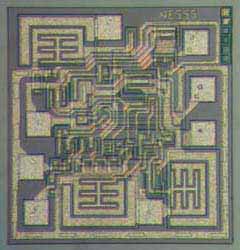
Substrate Thickness [mils] Die size mils [mm] Bonding pads Backside metallization Silicon 10 40.157 x 42.126 ±1 [1.02 x 1.07] min 3.74
x3.74 mils, 1µm thick, aluminium Backside of the die is coated with 0.5µm GOLD , which makes it compatible with AuSi or AuGe die attach.
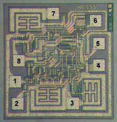
LM555 DIE LAYOUT - MECHANICAL SPECIFICATIONS LM555 DIE LAYOUT - MECHANICAL SPECIFICATIONS PAD # FUNCTION X(mils) X(mm) Y(mils) 1 GND 3.74
0.095 12.401 2 Trigger 4.527 0.115 4.921 3 Out 23.228 0.59 4.921 4 Reset 31.889 0.81 17.716 5 Control 30.708 0.78 32.677 6 Threshold 31.889
0.81 25 7 Discharge 16.535 0.42 35.236 8 Vcc 4.921 0.125 19.291 SEMICONDUCTOR ASSEMBLY PROCESS - SHORT APPLICATION NOTE Semiconix standard
bare die components are designed for thermosonic GOLD wire bonding and AuSi eutectic die attach. For AuSn or AuGe die attach process,
Ti/Pt/Au or Ti/Pd/Au are recommended backside metallization. For soft solder die attach, backside metallization may be any of Ti/Ni/Au,
Ti/Pt/Au, Ti/Pd/Au. For silver filled conductive epoxy die attach, AuSi as well as Ti/Ni/Au, Ti/Pt/Au, Ti/Pd/Au may be used. In general,
after die attach, prior to wire bonding operation an oxygen RF plasma clean operation is recommended. IMPORTANT NOTE: Aluminum wire should
not be used with gold pads due to potential reliability problem known as purple plague. Same it applies to Aluminum bonding pads with gold
wire! In the transition from SnPb solder to lead free and RoHS compliant packaging and assembly processes the reflow temperature has
increased in some cases from 180°C to 220°C. This may cause an increase of the rate of formation of gold aluminum intermetallic compounds
that are brittle and are conducive to increased contact resistance and or bond failure. See Application note AN-SMX-000. LM555 STANDARD
PRODUCTS PRICE LIST USM PART # MINIMUM ORDER QUANTITY Waffle Packs U/P($) USMLM555 100pc -WP $3.20 Products sold for space, military or
medical applications, element evaluation and/or level K or S qualification are subject to minimum order levels to be established on a case
by case basis. For any special applications, die level KGD qualification requirements, different packaging or custom configurations,
contact sales department. /cgi-bin/rfq.cgi" method="post" target="new"> INSTANT QUOTE Semiconix P/N Quantity E-mail DISCLAIMER - SEMICONIX
has made every effort to have this information as accurate as possible. However, no responsibility is assumed by SEMICONIX for its use, nor
for any infringements of rights of third parties, which may result from its use. SEMICONIX reserves the right to revise the content or
modify its product line without prior notice. SEMICONIX products are not authorized for and should not be used within support systems,
which are intended for surgical implants into the body, to support or sustain life, in aircraft, space equipment, submarine, or nuclear
facility applications without the specific written consent. HOME PRODUCT TREE PACKAGES /cgi-bin/getpdf.pl?part=SMXLM555&idx=12">PDF VERSION
SEARCH SEMICONIX SEMICONDUCTOR www.semiconix-semiconductor.com Tel:(408)986-8026 Fax:(408)986-8027 SEMICONIX SEMICONDUCTOR
Last updated: Display settings for best viewing: Current display settings: Page hits: Screen resolution: 1124x864 Screen resolution: Total
site visits: Color quality: 16 bit Color quality: bit © 1990- SEMICONIX SEMICONDUCTOR All rights reserved. No material from this site may
be used or reproduced without permission. Valid XHTML 1.0 Transitional by http://validator.w3.org
|


