|
Low Drop Voltage Regulators: SMS1085CD 3A LOW DROPOUT VOLTAGE REGULATOR same as AMS Advanced Monolithic Systems AMS1085CD, AMS Advanced Monolithic Systems AMS1085CD, AMS Advanced Monolithic Systems AMS1085CD TO263-3L AMS Advanced Monolithic Systems AMS1085CD manufactured by Semiconix Semiconductor - Gold chip technology for known good Low Drop Voltage Regulators die, Low Drop Voltage Regulators flip chip, Low Drop Voltage Regulators die, wafer foundry for discrete semiconductors, integrated circuits and integrated passive components from Semiconix Semiconductor
Low Drop Voltage Regulators: SMS1085CD 3A LOW DROPOUT VOLTAGE REGULATOR same as AMS Advanced Monolithic Systems AMS1085CD, AMS Advanced Monolithic Systems AMS1085CD, AMS Advanced Monolithic Systems AMS1085CD TO263-3L AMS Advanced Monolithic Systems AMS1085CD manufactured by Semiconix Semiconductor - Gold chip technology for known good Low Drop Voltage Regulators die, Low Drop Voltage Regulators flip chip, Low Drop Voltage Regulators die, wafer foundry for discrete semiconductors, integrated circuits and integrated passive components manufactured by Semiconix Semiconductor. Gold metallization for interconnections instead of aluminum or copper, for high reliability devices for system in package applications using silicon printed circuit boards, ceramic substrates or chip on board, assembled via flip chip or chip and wire.
TO263-3L AMS Advanced Monolithic Systems AMS1085CD, AMS Advanced Monolithic Systems AMS1085CD, AMS Advanced Monolithic Systems AMS1085CD AMS Advanced Monolithic Systems AMS1085CD,SMS1085CD,3A Low Drop Voltage Regulators,,Low Drop Voltage Regulators, gold,chip,goldchip,gold chip technology, known good die, flip chip, bare die, wafer foundry, discrete semiconductors, integrated circuits, integrated passive components,gold metallization, aluminum, copper, system in package, SIP, silicon printed circuit board, silicon PCB, ceramic substrates, chip on board, flip chip, chip and gold wire
Low Drop Voltage Regulators: SMS1085CD 3A LOW DROPOUT VOLTAGE REGULATOR same as AMS Advanced Monolithic
Systems AMS1085CD, AMS Advanced Monolithic Systems AMS1085CD, AMS Advanced Monolithic Systems AMS1085CD TO263-3L AMS
Advanced Monolithic Systems AMS1085CD manufactured by Semiconix Semiconductor - Gold chip technology for known good Low
Drop Voltage Regulators die, Low Drop Voltage Regulators flip chip, Low Drop Voltage Regulators die, wafer foundry for
discrete semiconductors, integrated circuits and integrated passive components from Semiconix Semiconductor Low Drop
Voltage Regulators: SMS1085CD 3A LOW DROPOUT VOLTAGE REGULATOR same as AMS Advanced Monolithic Systems AMS1085CD, AMS
Advanced Monolithic Systems AMS1085CD, AMS Advanced Monolithic Systems AMS1085CD TO263-3L AMS Advanced Monolithic
Systems AMS1085CD manufactured by Semiconix Semiconductor - Gold chip technology for known good Low Drop Voltage
Regulators die, Low Drop Voltage Regulators flip chip, Low Drop Voltage Regulators die, wafer foundry for discrete
semiconductors, integrated circuits and integrated passive components manufactured by Semiconix Semiconductor. Gold
metallization for interconnections instead of aluminum or copper, for high reliability devices for system in package
applications using silicon printed circuit boards, ceramic substrates or chip on board, assembled via flip chip or chip
and wire. TO263-3L AMS Advanced Monolithic Systems AMS1085CD, AMS Advanced Monolithic Systems AMS1085CD, AMS Advanced
Monolithic Systems AMS1085CD AMS Advanced Monolithic Systems AMS1085CD,SMS1085CD,3A Low Drop Voltage Regulators,,Low
Drop Voltage Regulators, gold,chip,goldchip,gold chip technology, known good die, flip chip, bare die, wafer foundry,
discrete semiconductors, integrated circuits, integrated passive components,gold metallization, aluminum, copper,
system in package, SIP, silicon printed circuit board, silicon PCB, ceramic substrates, chip on board, flip chip, chip
and gold wire REGISTER-LOGIN PRODUCTS CROSS REFERENCE INVENTORY REQUEST QUOTE ORDER ONLINE SITE MAP semiconix
semiconductor - where the future is today - gold chip technology SMS1085CD - BARE DIE GOLD CHIP TECHNOLOGY™ 3A LOW
DROPOUT VOLTAGE REGULATOR FEATURES APPLICATIONS 3A Low Drop Voltage Regulators - BARE DIE Three Terminal Adjustable or
Fixed Output Current of 10A Operates Down to 1V Dropout Line Regulation: 0.015% Load Regulation: 0.1% Load Regulation:
0.1% Available in TO220-3Lpackage. High reliability bare die Gold metallization RoHS compliant, Lead Free Compatible
with chip and wire assemblies High Efficiency Linear Regulators Post Regulators for Switching Supplies Microprocessor
Supply Battery Chargers Constant Current Regulators Notebook/Personal Computer Supplies Portable Instrumentation Chip
on Board System in package SIP Hybrid Circuits SMS1085CD AMS1085CD 3A LOW DROPOUT VOLTAGE REGULATOR Actual die layout
may vary 3A LOW DROPOUT VOLTAGE REGULATOR - PRODUCT DESCRIPTION SMS1085 series of adjustable and fixed voltage
regulators are designed to provide 3A output current and to operate down to 1V input-TOoutput differential. The dropout
voltage of the device is guaranteed maximum 1.5V at maximum output current, decreasing at lower load currents. On-chip
trimming adjusts the reference voltage to 1%. Current limit is also trimmed, minimizing the stress under overload
conditions on both the regulator and power source circuitry. The SMS1085 devices are pin compatible with older
three-terminal regulators and are offered in 3 lead TO220, 3 lead TO263 (Plastic DD) and TO252 (DPAK) packages. Low
Drop Voltage Regulators Integrated Circuits BD series products available in die form are ideal for high reliability
hybrid circuits and multi chip module applications. HIGH RELIABILITY BARE DIE AND SYSTEM IN PACKAGE - SHORT APPLICATION
NOTE COB (Chip on Board) and SiP (System-in-Package) are integrating proven mature products in bare die of mixed
technologies i.e. Si, GaAs, GaN, InP, passive components, etc that cannot be easily implemented in SOC (System-on-Chip)
technology. COB and SiP have small size footprint, high density, shorter design cycle time, easier to redesign and
rework, use simpler and less expensive assembly process. For extreme applications the bare die has to withstand also
harsh environmental conditions without the protection of a package. KGD, Known Good Die concept is no longer
satisfactory if the die cannot withstand harsh environmental conditions and degrades. Standard semiconductor devices
supplied by many manufacturers in bare die are build with exposed aluminum pads that are extremely sensitive to
moisture and corrosive components of the atmosphere. Semiconix has reengineered industry standard products and now
offers known good die for bare die applications with gold interconnection and well-engineered materials that further
enhance the die reliability. Semiconix also offers Silicon Printed Circuit Board technology with integrated passive
components as a complete high reliability SIP solution for medical, military and space applications. See AN-SMX-001
DISCRETE SEMICONDUCTORS MANUFACTURING PROCESS Discrete semiconductors are manufactured using Semiconix in house high
reliability semiconductor manufacturing processes. All semiconductor devices employ precision doping via ion
implantation, silicon nitride junction passivation, platinum silicided contacts and gold interconnect metallization for
best performance and reliability. MNOS capacitors, Tantalum Nitride TaN or Sichrome SiCr thin film resistors are easily
integrated with discrete semiconductors on same chip to obtain standard and custom complex discrete device solutions.
ABSOLUTE MAXIMUM RATINGS @ 25 °C (unless otherwise stated) Parameter Symbol Value Unit Power Dissipation Internally
limited Input Voltage 15 V Storage Temperature -65 to +150 °C Control Section 0° C to 125 °C Power Transistor 0° C to
150 ° C Electrical Characteristics* at IOUT=0 mA, TC=25°C unless otherwise noted Name Symbol Test Conditions Value Unit
Min. Typ. Max Reference Voltage (Note 2) IOUT=10 mA 1.238 1.25 1.262 V Reference Voltage over the full operating
temperature range. 10mA≤IOUT≤3A, 1.5V≤ (VIN - VOUT)≤12V 1.225 1.25 1.27 V Line Regulation ILOAD=10 mA, 1.5V≤ (VIN -
VOUT)≤12V 0.3 6 mV Line Regulation, over the full operating temperature range. ILOAD=10 mA, 1.5V≤ (VIN - VOUT)≤12V 0.6
10 mV Load Regulation, (Notes 2, 3) (VIN - VOUT)=3V, 10mA≤IOUT≤3A 0.1 0.3 % Load Regulation, over the full operating
temperature range. (VIN - VOUT)=3V, 10mA≤IOUT≤3A 0.2 0.4 % Dropout Voltage (VIN - VOUT) ∆VOUT, ∆VREF=1%, IOUT=3 A (Note
4) 1.3 1.5 V Current Limit (VIN - VOUT)=5V 3 3.5 4 A Minimum Load Current (VIN - VOUT)=12V (Note 5) 5 10 mA Quiescent
Current VIN≤12V 5 10 mA Ripple Rejection f=120Hz, COUT=25µF Tantalum, IOUT=3A, (VIN-VOUT )=3V, CADJ=25µF 60 75 dB
Thermal Regulation TA=25°C, 30ms pulse 0.008 0.04 %W Adjust Pin Current 10mA≤IOUT≤3A, 1.5V≤ (VIN - VOUT)≤12V 55 m A
Adjust Pin Current, over the full operating temperature range. 10mA≤IOUT≤3A, 1.5V≤ (VIN - VOUT)≤12V 120 m A Adjust Pin
Current Change 10mA≤IOUT≤3A, 1.5V≤ (VIN - VOUT)≤12V 0.2 5 m A Temperature Stability 0.5 % Long Term Stability TA=125°C,
1000Hrs 0.3 1 % RMS Output Noise (% of VOUT ) TA=25°C, 10Hz≤f≤10kHz 0.003 % Thermal Resistance Junction-to-Case M
Package: Control Circuitry/ Power Transistor 1.5/4.0 °C/W Thermal Resistance Junction-to-Case T Package: Control
Circuitry/ Power Transistor 1.5/4.0 °C/W Note 1: Absolute Maximum Ratings indicate limits beyond which damage to the
device may occur. For guaranteed specifications and test conditions, see the Electrical Characteristics. The guaranteed
specifications apply only for the test conditions listed. Note 2: Line and Load regulation are guaranteed up to the
maximum power dissipation of 15W. Power dissipation is determined by the input/output differential and the output
current. Guaranteed maximum power dissipation will not be available over the full input/output range. Note 3:See
thermal regulation specifications for changes in output voltage due to heating effects. Line and load regulation are
measured at a constant junction temperature by low duty cycle pulse testing. Load regulation is measured at the output
lead ~1/8” from the package. Note 4: Dropout voltage is specified over the full output current range of the device.
Note 5: Minimum load current is defined as the minimum output current required to maintain regulation. When (VIN -
VOUT) = 12V the device is guaranteed to regulate if the output current is greater than 10mA. SPICE MODEL AMS1085CD
spice model pending. CROSS REFERENCE PARTS: AMS Advanced Monolithic Systems AMS1085CD, AMS Advanced Monolithic Systems
AMS1085CD, AMS Advanced Monolithic Systems AMS1085CD GENERAL DIE INFORMATION Substrate Thickness [mils] Die size [mils]
Bonding pads Backside metallization Silicon Si 10 1 122x130±1 [3.1x3.3±0.025] Pads are minimum 4x4mils, 3µm thick,
99.99% electroplated gold with a TiW barrier that withstands 30 min at 400°C in air without loss of adhesion. P/N Metal
Die attach process -BD0 Au/Si Au/Si eutectic -BD1 Ti/Pd/Au AuSn,AuGe -BD2 Ti/Pt/Au AuSn,AuGe -BD3 Ti/Ni/Au Soft Solder
SAC -BD4 Ti/Pt/AuSn AuSn eutectic LAYOUT / DIMENSIONS / PAD LOCATIONS Actual die layout may vary SMS1085CD AMS Advanced
Monolithic Systems AMS1085CD, AMS Advanced Monolithic Systems AMS1085CD, AMS Advanced Monolithic Systems AMS1085CD AMS
Advanced Monolithic Systems AMS1085CD 3A LOW DROPOUT VOLTAGE REGULATOR SMS1085CD AMS1085CD 3A LOW DROPOUT VOLTAGE
REGULATOR Pad locations Pin # Function X [µm] Y [µm] X [mils] Y [mils] 1 Vin 1535 1286 60.43 50.63 2 Vin 1535 2727
60.43 107.36 3 Vout 419 2014 16.50 79.29 4 Vout 2589 2014 101.93 79.29 5 ADJ 279 899 10.98 35.39 SMS1085CD AMS Advanced
Monolithic Systems AMS1085CD, AMS Advanced Monolithic Systems AMS1085CD, AMS Advanced Monolithic Systems AMS1085CD AMS
Advanced Monolithic Systems AMS1085CD 3A LOW DROPOUT VOLTAGE REGULATOR APPLICATION HINTS APPLICATION HINTS The SMS1085
series of adjustable and fixed regulators are easy to use and have all the protection features expected in high
performance voltage regulators: short circuit protection and thermal shutdown. Pin compatible with older three terminal
adjustable regulators, these devices offer the advantage of a lower dropout voltage, more precise reference tolerance
and improved reference stability with temperature. Stability The circuit design used in the SMS1085 series requires the
use of an output capacitor as part of the device frequency compensation. The addition of 150µF aluminum electrolytic or
a 22µF solid tantalum on the output will ensure stability for all operating conditions. When the adjustment terminal is
bypassed to improve the ripple rejection, the requirement for an output capacitor increases. The value of 22µF tantalum
or 150µF aluminum covers all cases of bypassing the adjustment terminal. Without bypassing the adjustment terminal
smaller capacitors can be used with equally good results. To ensure good transient response with heavy load current
changes capacitor values on the order of 100µF are used in the output of many regulators. To further improve stability
and transient response of these devices larger values of output capacitor can be used. Protection Diodes Unlike older
regulators, the SMS1085 family does not need any protection diodes between the adjustment pin and the output and from
the output to the input to prevent over-stressing the die. Internal resistors are limiting the internal current paths
on the SMS1085 adjustment pin, therefore even with capacitors on the adjustment pin no protection diode is needed to
ensure device safety under short-circuit conditions. Diodes between the input and output are not usually needed.
Microsecond surge currents of 50A to 100A can be handled by the internal diode between the input and output pins of the
device. In normal operations it is difficult to get those values of surge currents even with the use of large output
capacitances. If high value output capacitors are used, such as 1000µF to 5000µF and the input pin is instantaneously
shorted to ground, damage can occur. A diode from output to input is recommended, when a crowbar circuit at the input
of the SMS1085 is used. Normal power supply cycling or even plugging and unplugging in the system will not generate
current large enough to do any damage. The adjustment pin can be driven on a transient basis ±25V, with respect to the
output without any device degradation. As with any IC regulator, none the protection circuitry will be functional and
the internal transistors will break down if the maximum input to output voltage differential is exceeded. Overload
Recovery When the power is first turned on, as the input voltage rises, the output follows the input, permitting the
regulator to start up into heavy loads. During the start-up, as the input voltage is rising, the input-to-output
voltage differential remains small, allowing the regulator to supply large output currents. A problem can occur with a
heavy output load when the input voltage is high and the output voltage is low, when the removal of an output short
will not permit the output voltage to recover. The load line for such a load may intersect two points on the output
current curve. In this case, there are two stable output operating points for the regulator. With this double
intersection, the power supply may need to be cycled down to zero and brought up again to make the output recover.
Ripple Rejection The ripple rejection values are measured with the adjustment pin bypassed. The impedance of the adjust
pin capacitor at the ripple frequency should be less than the value of R1 (normally 100. to120.) for a proper bypassing
and ripple rejection approaching the values shown. The size of the required adjust pin capacitor is a function of the
input ripple frequency. If R1=100. at 120Hz the adjust pin capacitor should be 25µF. At 10kHz only 0.22µF is needed.
The ripple rejection will be a function of output voltage, in circuits without an adjust pin bypass capacitor. The
output ripple will increase directly as a ratio of the output voltage to the reference voltage (VOUT / VREF ). Output
Voltage The SMS1085 series develops a 1.25V reference voltage between the output and the adjust terminal. Placing a
resistor between these two terminals causes a constant current to flow through R1 and down through R2 to set the
overall output voltage. This current is normally the specified minimum load current of 10mA. Because IADJ is very small
and constant it represents a small error and it can usually be ignored. VOUT = VREF (1+ R2/R1)+IADJR2 Load Regulation
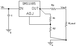
True remote load sensing it is not possible to provide, because the SMS1085 is a three terminal device. The resistance
of the wire connecting the regulator to the load will limit the load regulation. The data sheet specification for load
regulation is measured at the bottom of the package. Negative side sensing is a true Kelvin connection, with the bottom
of the output divider returned to the negative side of the load. The best load regulation is obtained when the top of
the resistor divider R1 is connected directly to the case not to the load. If R1 were connected to the load, the
effective resistance between the regulator and the load would be: RP x ( R2+R1 ) , RP = Parasitic Line Resistance
*CONNECT R1 TO CASE, CONNECT R2 TO LOAD Connected as shown, RP is not multiplied by the divider ratio. Using 16-gauge
wire the parasitic line resistance is about 0.004. per foot, translating to 4mV/ft at 1A load current. It is important
to keep the positive lead between regulator and load as short as possible and use large wire or PC board traces.
Thermal Considerations The SMS1085 series have internal power and thermal limiting circuitry designed to protect the
device under overload conditions. However maximum junction temperature ratings should not be exceeded under continuous
normal load conditions. Careful consideration must be given to all sources of thermal resistance from junction to
ambient, including junction-to-case, case-to-heat sink interface and heat sink resistance itself. To ensure safe
operating temperatures and reflect more accurately the device temperature, new thermal resistance specifications have
been developed. Unlike older regulators with a single junction-to-case thermal resistance specification, the data
section for these new regulators provides a separate thermal resistance and maximum junction temperature for both the
Control Section and the Power Transistor. Calculations for both temperatures under certain conditions of ambient
temperature and heat sink resistance and to ensure that both thermal limits are met. Junction-to-case thermal
resistance is specified from the IC junction to the bottom of the case directly below the die. This is the lowest
resistance path for the heat flow. In order to ensure the best possible thermal flow from this area of the package to
the heat sink proper mounting is required. Thermal compound at the case-to-heat sink interface is recommended. A
thermally conductive spacer can be used, if the case of the device must be electrically isolated, but its added
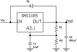
contribution to thermal resistance has to be considered. Vout Basic Adjustable Regulator Figure 1: Vout Basic
Adjustable Regulator Protection diodes Figure 2: Protection diodes Connections for Best Load Regulation Figure 3:
Connections for Best Load Regulation SEMICONDUCTOR ASSEMBLY PROCESS - SHORT APPLICATION NOTE Semiconix standard bare
die components are designed for thermosonic GOLD wire bonding and AuSi eutectic die attach. For AuSn or AuGe die attach
process, Ti/Pt/Au or Ti/Pd/Au are recommended backside metallization. For soft solder die attach, backside
metallization may be any of Ti/Ni/Au, Ti/Pt/Au, Ti/Pd/Au. For silver filled conductive epoxy die attach, AuSi as well
as Ti/Ni/Au, Ti/Pt/Au, Ti/Pd/Au may be used. In general, after die attach, prior to wire bonding operation an oxygen RF
plasma clean operation is recommended. IMPORTANT NOTE: Aluminum wire should not be used with gold pads due to potential
reliability problem known as purple plague. Same it applies to Aluminum bonding pads with gold wire! In the transition
from SnPb solder to lead free and RoHS compliant packaging and assembly processes the reflow temperature has increased
in some cases from 180°C to 220°C. This may cause an increase of the rate of formation of gold aluminum intermetallic
compounds that are brittle and are conducive to increased contact resistance and or bond failure. See Application note
AN-SMX-000. STANDARD PRODUCTS ORDERING INFORMATION SMS P/N WAFFLE PACKS QUANTITY U/P($) FILM FRAME MIN QUANTITY U/P($)
SMS1085CD-BD -WP 1000 -FF 1000 SMS1085CD-BD -WP 5000 -FF 5000 PRICES - Listed prices are only for standard products,
available from stock. Inventory is periodically updated. List prices for other quantities and tolerances are available
on line through Instant Quote. For standard products available from stock, there is a minimum line item order of
$550.00. No rights can be derived from pricing information provided on this website. Such information is indicative
only, for budgetary use only and subject to change by SEMICONIX SEMICONDUCTOR at any time and without notice. LEAD
TIMES - Typical delivery for standard products is 4-6 weeks ARO. For custom devices consult factory for an update on
minim orders and lead times. CONTINOUS SUPPLY - Semiconix guarantees continuous supply and availability of any of its
standard products provided minimum order quantities are met. CUSTOM PRODUCTS - For custom products sold as tested, bare
die or known good die KGD, there will be a minimum order quantity MOQ. Dice are 100% functional tested, visual
inspected and shipped in antistatic waffle packs. For high volume and pick and place applications, dice are also
shipped on film frame -FF. For special die level KGD requirements, different packaging or custom configurations,
contact sales via CONTACTS page. SAMPLES - Samples are available only for customers that have issued firm orders
pending qualification of product in a particular application. ORDERING - Semiconix accepts only orders placed on line
by registered customers. On line orders are verified, accepted and acknowledged by Semiconix sales department in
writing. Accepted orders are non cancelable binding contracts. SHIPING - Dice are 100% functional tested, visual
inspected and shipped in antistatic waffle packs. For high volume and pick and place applications, dice are also
shipped on film frame -FF. INSTANT QUOTE Semiconix P/N Quantity E-mail DISCLAIMER - SEMICONIX has made every effort to
have this information as accurate as possible. However, no responsibility is assumed by SEMICONIX for its use, nor for
any infringements of rights of third parties, which may result from its use. SEMICONIX reserves the right to revise the
content or modify its product line without prior notice. SEMICONIX products are not authorized for and should not be
used within support systems, which are intended for surgical implants into the body, to support or sustain life, in
aircraft, space equipment, submarine, or nuclear facility applications without the specific written consent. HOME
PRODUCT TREE PACKAGES PDF VERSION SEARCH SEMICONIX SEMICONDUCTOR www.semiconix-semiconductor.com
Tel:(408)986-8026 Fax:(408)986-8027 SEMICONIX SEMICONDUCTOR Last updated:January 01, 1970 Display settings for best
viewing: Current display settings: Page hits: 1 Screen resolution: 1124x864 Screen resolution: Total site visits: 1
Color quality: 16 bit Color quality: bit © 1990-2009 SEMICONIX SEMICONDUCTOR All rights reserved. No material from this
site may be used or reproduced without permission.
|