| REGISTER-LOGIN | PRODUCTS | CROSS REFERENCE | INVENTORY | REQUEST QUOTE | ORDER ONLINE | SITE MAP |
| SMS5105S - BARE DIE | |
| GOLD CHIP TECHNOLOGY™ | 500mA CMOS LOW DROPOUT VOLTAGE REGULATOR |
| FEATURES | APPLICATIONS | 500mA CMOS LOW DROPOUT VOLTAGE REGULATOR - BARE DIE | |
|
Fixed and Adjustable Versions Available Output Current up to 500mA Very Low Quiescent Current Input-output Differential less than 0.5V Short Circuit Protection Internal Thermal Overload Protection ENABLE Pin available in selected packages High reliability bare die Gold metallization RoHS compliant, Lead Free Compatible with chip and wire assemblies |
Cellular Telephones Portable Consumer Equipment Portable (Notebook) Computers Battery Powered Systems Portable Instrumentation Radio Control Systems CD/DVD drives Chip on Board System in package SIP Hybrid Circuits |

|
| 500mA CMOS LOW DROPOUT VOLTAGE REGULATOR - PRODUCT DESCRIPTION |
|
SMS5105 series consists of positive fixed and adjustable voltage regulators ideally suited for use in battery-powered systems. These devices feature very low quiescent current (500uA or less) when supplying loads up to 500mA, and a standby current less than 500nA when disabled using the ENABLE pin (available in selected packages). These unique characteristics and the low input-output differential required for proper regulation (0.5V for output currents of 500mA) make the SMS5105 ideal for use in standby power systems. Internal current limiting and thermal shutdown features provide protection for all SMS5105 series devices regardless of package type. The SMS5105 is offered as fixed voltage regulators in the 5 lead SOT-23, SOT-89, SOT-223, and 8 lead SOIC packages, and as adjustable voltage regulators in the 5 lead SOT-23 and 8 lead SOIC packages. All devices in the 5 lead SOT-23 and 8 lead SOIC packages are provided with ENABLE pin. Low Drop Voltage Regulators Integrated Circuits BD series products available in die form are ideal for high reliability hybrid circuits and multi chip module applications. |
| HIGH RELIABILITY BARE DIE AND SYSTEM IN PACKAGE - SHORT APPLICATION NOTE |
| COB (Chip on Board) and SiP (System-in-Package) are integrating proven mature products in bare die of mixed technologies i.e. Si, GaAs, GaN, InP, passive components, etc that cannot be easily implemented in SOC (System-on-Chip) technology. COB and SiP have small size footprint, high density, shorter design cycle time, easier to redesign and rework, use simpler and less expensive assembly process. For extreme applications the bare die has to withstand also harsh environmental conditions without the protection of a package. KGD, Known Good Die concept is no longer satisfactory if the die cannot withstand harsh environmental conditions and degrades. Standard semiconductor devices supplied by many manufacturers in bare die are build with exposed aluminum pads that are extremely sensitive to moisture and corrosive components of the atmosphere. Semiconix has reengineered industry standard products and now offers known good die for bare die applications with gold interconnection and well-engineered materials that further enhance the die reliability. Semiconix also offers Silicon Printed Circuit Board technology with integrated passive components as a complete high reliability SIP solution for medical, military and space applications. See AN-SMX-001 |
| DISCRETE SEMICONDUCTORS MANUFACTURING PROCESS |
| Discrete semiconductors are manufactured using Semiconix in house high reliability semiconductor manufacturing processes. All semiconductor devices employ precision doping via ion implantation, silicon nitride junction passivation, platinum silicided contacts and gold interconnect metallization for best performance and reliability. MNOS capacitors, Tantalum Nitride TaN or Sichrome SiCr thin film resistors are easily integrated with discrete semiconductors on same chip to obtain standard and custom complex discrete device solutions. |
| ABSOLUTE MAXIMUM RATINGS @ 25 °C (unless otherwise stated) | |||
| Parameter | Symbol | Value | Unit |
| Power Dissipation | Internally Limited | ||
| Input Voltage | -0.3 to +6.5 | V | |
| Overvoltage Protection | 26 to 40 | V | |
| Storage Temperature | -65 to +150 | °C | |
| Operating Junction Temperature | 125 | ° C | |
| Operating Temperature Range | -25 to 125 | ° C | |
| Electrical Characteristics* at VIN=6V, VOUT=3V, IOUT=1mA, TJ=25°C, COUT=2.2µF unless otherwise specified. | ||||||
| Name | Symbol | Test Conditions | Value | Unit | ||
| Min. | Typ. | Max | ||||
| Reference Voltage | 1.231 | 1.25 | 1.269 | V | ||
| Reference Voltage over the full operating temperature range. | IOUT≤100 mA, -25°C≤TJ≤125°C,Measured from FB pin to GROUND | 1.218 | 1.25 | 1.282 | V | |
| Output Voltage | 1.25 | 5 | V | |||
| Line Regulation | VOUT + 1V≤VIN≤6V | - | 1.5 | % | ||
| Load Regulation | 1mA≤IO≤100 mA | 0.3 | 1 | % | ||
| Load Regulation | 5mA≤IO≤500 mA | 1 | 2 | % | ||
| Dropout Voltage (VIN - VOUT) | IOUT≤10 mA | 20 | 25 | mV | ||
| Dropout Voltage (VIN - VOUT) | IOUT=100 mA | 100 | 125 | mV | ||
| Dropout Voltage (VIN - VOUT) | IOUT=500 mA (Note 5) | 400 | 500 | mV | ||
| Quiescent Current | IOUT=10 mA | 350 | 450 | µ A | ||
| Quiescent Current | IOUT=100 mA | 350 | 450 | µ A | ||
| Quiescent Current | IOUT=500 mA | 350 | 450 | µ A | ||
| Quiescent Current | RL=500Ω, In disabled state, VENABLE=0 | 100 | 500 | nA | ||
| Maximum Operational Input Voltage | 6 | V | ||||
| ENABLE Threshold Current | VENABLE=0.6 x VIN, VIN=3V to 6V | 0.01 | 1 | nA | ||
| ENABLE Threshold Voltage | Enabled VIN=3V to 6V (Note 6) | 60 | % VIN | |||
| ENABLE Threshold Voltage | Disabled VIN=3V to 6V (Note 6) | 15 | % VIN | |||
| Wake-Up Response Time (from disabled state) | Note 7 | 20 | 30 | µs | ||
|
Note 1: Absolute Maximum Ratings are limits beyond which damage to the device may occur. For guaranteed performance limits and associated test conditions, see the Electrical Characteristics tables. Note 2: To ensure constant junction temperature, low duty cycle pulse testing is used. Note 3: Limits appearing in boldface type apply over the entire junction temperature range for operation. Limits appearing in normal type apply for TA = TJ = 25°C. Note 4: The maximum allowable power dissipation is a function of the maximum junction temperature TJ(MAX), the junction-to ambient thermal resistance θJ-A and the ambient temperature TA. The maximum allowable power dissipation at any ambient temperature is calculated using: Where the values of the junction-to-ambient thermal resistances are as follows: 220°C/W for SOT-23-5 (M1) and 160°C/W for the molded plastic SO-8 (S). Note 5: Dropout Voltage is defined as the input to output differential at which the output voltage drops 100mV below its nominal value measured at 1V differential. Note 6: ENABLE Threshold Voltage levels are specified as a percentage of input voltage VIN. Quiescent current can be minimized by choosing VENABLE HIGH equal to VIN. Note 7: Time required for VOUT to reach 95% of output voltage setting after VENABLE is switched from 0V to VIN. |
||||||
| SPICE MODEL | ||||||
| Spice model pending. | ||||||
| CROSS REFERENCE PARTS: AMS Advanced Monolithic Systems AMS5105S, AMS Advanced Monolithic Systems AMS5105S | ||||||
| GENERAL DIE INFORMATION | ||||||||||||||||||||||
| Substrate | Thickness [mils] |
Die size [mils] |
Bonding pads | Backside metallization | ||||||||||||||||||
| Silicon Si |
10 1 |
101x62±1 [2.57x1.57±0.025] |
Pads are minimum 4x4mils, 3µm thick, 99.99% electroplated gold with a TiW barrier that withstands 30 min at 400°C in air without loss of adhesion. |
|
||||||||||||||||||
| LAYOUT / DIMENSIONS / PAD LOCATIONS | ||||||||||||||||||||||||||||||||||||||||
|
||||||||||||||||||||||||||||||||||||||||

|
|
|||||||||||||||||||||||||||||||||||||||
|
||||||||||||||||||||||||||||||||||||||||

|
||||||||||||||||||||||||||||||||||||||||
| APPLICATION HINTS |
Pin Description |
|
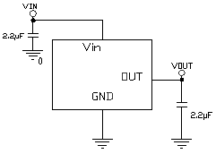
| Figure 1: Typical Application - Adjustable Output |
 |
| Figure 2: Typical Application - Fixed Output |
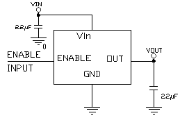 |
| Figure 3: Typical Application - Fixed Output with Enable |
 |
| Figure 4: Single Supply Comparator with Temperature Compensated Threshold |
 |
| Figure 5: Series Regulator |
 |
| Figure 6: Higher Current Shunt Regulator |
 |
| Figure 7: Current Limiter or Current Source |
 |
| Figure 8: Constant Current Sink |
 |
| Figure 9: Over/Under Voltage Protection Circuit |
 |
| Figure 10: Delay timer |
| SEMICONDUCTOR ASSEMBLY PROCESS - SHORT APPLICATION NOTE |
|
Semiconix standard bare die components are designed for thermosonic GOLD wire bonding and AuSi eutectic die attach. For AuSn or AuGe die
attach process, Ti/Pt/Au or Ti/Pd/Au are recommended backside metallization. For soft solder die attach, backside metallization may be any of Ti/Ni/Au, Ti/Pt/Au, Ti/Pd/Au. For silver filled conductive epoxy die attach, AuSi as well as Ti/Ni/Au, Ti/Pt/Au, Ti/Pd/Au may be used. In general, after die attach, prior to wire bonding operation an oxygen RF plasma clean operation is recommended. IMPORTANT NOTE: Aluminum wire should not be used with gold pads due to potential reliability problem known as purple plague. Same it applies to Aluminum bonding pads with gold wire! In the transition from SnPb solder to lead free and RoHS compliant packaging and assembly processes the reflow temperature has increased in some cases from 180°C to 220°C. This may cause an increase of the rate of formation of gold aluminum intermetallic compounds that are brittle and are conducive to increased contact resistance and or bond failure. See Application note AN-SMX-000. |
| STANDARD PRODUCTS ORDERING INFORMATION |
| SMS P/N | WAFFLE PACKS | QUANTITY | U/P($) | FILM FRAME | MIN QUANTITY | U/P($) |
| SMS5105S-BD | -WP | 1000 | -FF | 1000 | ||
| SMS5105S-BD | -WP | 5000 | -FF | 5000 |
| PRICES - Listed prices are only for standard products, available from stock. Inventory is periodically updated. List prices for other quantities and tolerances are available on line through Instant Quote. For standard products available from stock, there is a minimum line item order of $550.00. No rights can be derived from pricing information provided on this website. Such information is indicative only, for budgetary use only and subject to change by SEMICONIX SEMICONDUCTOR at any time and without notice. |
| LEAD TIMES - Typical delivery for standard products is 4-6 weeks ARO. For custom devices consult factory for an update on minim orders and lead times. |
| CONTINOUS SUPPLY - Semiconix guarantees continuous supply and availability of any of its standard products provided minimum order quantities are met. |
| CUSTOM PRODUCTS - For custom products sold as tested, bare die or known good die KGD, there will be a minimum order quantity MOQ. Dice are 100% functional tested, visual inspected and shipped in antistatic waffle packs. For high volume and pick and place applications, dice are also shipped on film frame -FF. For special die level KGD requirements, different packaging or custom configurations, contact sales via CONTACTS page. |
| SAMPLES - Samples are available only for customers that have issued firm orders pending qualification of product in a particular application. |
| ORDERING - Semiconix accepts only orders placed on line by registered customers. On line orders are verified, accepted and acknowledged by Semiconix sales department in writing. Accepted orders are non cancelable binding contracts. |
| SHIPING - Dice are 100% functional tested, visual inspected and shipped in antistatic waffle packs. For high volume and pick and place applications, dice are also shipped on film frame -FF. |
| DISCLAIMER - SEMICONIX has made every effort to have this information as accurate as possible. However, no responsibility is assumed by SEMICONIX for its use, nor for any infringements of rights of third parties, which may result from its use. SEMICONIX reserves the right to revise the content or modify its product line without prior notice. SEMICONIX products are not authorized for and should not be used within support systems, which are intended for surgical implants into the body, to support or sustain life, in aircraft, space equipment, submarine, or nuclear facility applications without the specific written consent. |
| HOME | PRODUCT TREE | PACKAGES | PDF VERSION | SEARCH |
| SEMICONIX SEMICONDUCTOR | www.semiconix-semiconductor.com Tel:(408)758-8694 Fax:(408)986-8027 |
SEMICONIX SEMICONDUCTOR |
| Last updated:July 06, 2009 | Display settings for best viewing: | Current display settings: |
| Page hits: 103 | Screen resolution: 1124x864 | Screen resolution: |
| Total site visits: 21101150 | Color quality: 16 bit | Color quality: bit |
| © 1990-2024 SEMICONIX SEMICONDUCTOR All rights reserved. No material from this site may be used or reproduced without permission. | ||