|
Low Drop Voltage Regulators: SMS1505CTV-3.5V 5A LOW DROPOUT VOLTAGE REGULATORS same as AMS Advanced Monolithic Systems AMS1505CTV-3.5V, AMS Advanced Monolithic Systems AMS1505CTV-3.5V TO220-5L AMS Advanced Monolithic Systems AMS1505CTV-3.5V manufactured by Semiconix Semiconductor - Gold chip technology for known good Low Drop Voltage Regulators die, Low Drop Voltage Regulators flip chip, Low Drop Voltage Regulators die, wafer foundry for discrete semiconductors, integrated circuits and integrated passive components from Semiconix Semiconductor
Low Drop Voltage Regulators: SMS1505CTV-3.5V 5A LOW DROPOUT VOLTAGE REGULATORS same as AMS Advanced Monolithic Systems AMS1505CTV-3.5V, AMS Advanced Monolithic Systems AMS1505CTV-3.5V TO220-5L AMS Advanced Monolithic Systems AMS1505CTV-3.5V manufactured by Semiconix Semiconductor - Gold chip technology for known good Low Drop Voltage Regulators die, Low Drop Voltage Regulators flip chip, Low Drop Voltage Regulators die, wafer foundry for discrete semiconductors, integrated circuits and integrated passive components manufactured by Semiconix Semiconductor. Gold metallization for interconnections instead of aluminum or copper, for high reliability devices for system in package applications using silicon printed circuit boards, ceramic substrates or chip on board, assembled via flip chip or chip and wire.
TO220-5L AMS Advanced Monolithic Systems AMS1505CTV-3.5V, AMS Advanced Monolithic Systems AMS1505CTV-3.5V AMS Advanced Monolithic Systems AMS1505CTV-3.5V,SMS1505CTV-3.5V,5A Low Drop Voltage Regulators,,Low Drop Voltage Regulators, gold,chip,goldchip,gold chip technology, known good die, flip chip, bare die, wafer foundry, discrete semiconductors, integrated circuits, integrated passive components,gold metallization, aluminum, copper, system in package, SIP, silicon printed circuit board, silicon PCB, ceramic substrates, chip on board, flip chip, chip and gold wire
Low Drop Voltage Regulators: SMS1505CTV-3.5V 5A LOW DROPOUT VOLTAGE REGULATORS same as AMS Advanced Monolithic
Systems AMS1505CTV-3.5V, AMS Advanced Monolithic Systems AMS1505CTV-3.5V TO220-5L AMS Advanced Monolithic Systems
AMS1505CTV-3.5V manufactured by Semiconix Semiconductor - Gold chip technology for known good Low Drop Voltage
Regulators die, Low Drop Voltage Regulators flip chip, Low Drop Voltage Regulators die, wafer foundry for discrete
semiconductors, integrated circuits and integrated passive components from Semiconix Semiconductor Low Drop Voltage
Regulators: SMS1505CTV-3.5V 5A LOW DROPOUT VOLTAGE REGULATORS same as AMS Advanced Monolithic Systems AMS1505CTV-3.5V,
AMS Advanced Monolithic Systems AMS1505CTV-3.5V TO220-5L AMS Advanced Monolithic Systems AMS1505CTV-3.5V manufactured
by Semiconix Semiconductor - Gold chip technology for known good Low Drop Voltage Regulators die, Low Drop Voltage
Regulators flip chip, Low Drop Voltage Regulators die, wafer foundry for discrete semiconductors, integrated circuits
and integrated passive components manufactured by Semiconix Semiconductor. Gold metallization for interconnections
instead of aluminum or copper, for high reliability devices for system in package applications using silicon printed
circuit boards, ceramic substrates or chip on board, assembled via flip chip or chip and wire. TO220-5L AMS Advanced
Monolithic Systems AMS1505CTV-3.5V, AMS Advanced Monolithic Systems AMS1505CTV-3.5V AMS Advanced Monolithic Systems
AMS1505CTV-3.5V,SMS1505CTV-3.5V,5A Low Drop Voltage Regulators,,Low Drop Voltage Regulators, gold,chip,goldchip,gold
chip technology, known good die, flip chip, bare die, wafer foundry, discrete semiconductors, integrated circuits,
integrated passive components,gold metallization, aluminum, copper, system in package, SIP, silicon printed circuit
board, silicon PCB, ceramic substrates, chip on board, flip chip, chip and gold wire REGISTER-LOGIN PRODUCTS CROSS
REFERENCE INVENTORY REQUEST QUOTE ORDER ONLINE SITE MAP semiconix semiconductor - where the future is today - gold chip
technology SMS1505CTV-3.5V - nanoDFN GOLD CHIP TECHNOLOGY™ TO220-5L 5A LOW DROPOUT VOLTAGE REGULATORS FEATURES
APPLICATIONS 5A Low Drop Voltage Regulators - nDFN Adjustable or Fixed Output 1.5V, 2.5V, 2.85V, 3.0V, 3.3V, 3.5V and
5.0V Output Current of 1.5A Low Dropout, 500mV at 1.5A Output Current Fast Transient Response Remote Sense High
reliability nanoDFN package Unique 10mils thin design Gold over nickel metallization RoHS compliant, Lead Free
Compatible with surface mount, chip and wire and flip chip assembly process. Available packaged in TO220-5L High
Current Regulators Post Regulators for Switching Supplies Adjustable Power Supply Notebook/Personal Computer Supplies
Chip on Board System in package SIP Hybrid Circuits SMS1505CTV-3.5V AMS1505CTV-3.5V 5A LOW DROPOUT VOLTAGE REGULATORS
5A LOW DROPOUT VOLTAGE REGULATORS - PRODUCT DESCRIPTION SMS1505 series of adjustable and fixed low dropout voltage
regulators are designed to provide 5A output current to power the new generation of microprocessors. The dropout
voltage of the device is 100mV at light loads and rising to 500mV at maximum output current. A second low current input
voltage 1V or greater then the output voltage is required to achieve this dropout. The SMS1505 can also be used as a
single supply device. New features have been added to the SMS1505: a remote Sense pin is brought out virtually
eliminating output voltage variations due to load changes. The typical load regulation, measured at the Sense pin, for
a load current step of 100mA to 5A is less than 1mV. The SMS1505 series has fast transient response. The Adjust pin is
brought out on fixed devices. To further improve the transient response the addition of a small capacitor on the Adjust
pin is recommended. The SMS1505 series are ideal for generating processor supplies of 2V to 3V on motherboards where
both 5V and 3.3V supplies are available. The SMS1505 devices are offered in 5 lead TO-220, 5L TO-263 (plastic DD) and
5L TO-252 (DPAK) packages. Semiconix Low Drop Voltage Regulators Integrated Circuits series are available in very thin
0201 nanoDFN package. These products are ideal for surface mount, hybrid circuits and multi chip module applications.
HIGH RELIABILITY BARE DIE AND SYSTEM IN PACKAGE - SHORT APPLICATION NOTE COB (Chip on Board) and SiP
(System-in-Package) are integrating proven mature products in bare die of mixed technologies i.e. Si, GaAs, GaN, InP,
passive components, etc that cannot be easily implemented in SOC (System-on-Chip) technology. COB and SiP have small
size footprint, high density, shorter design cycle time, easier to redesign and rework, use simpler and less expensive
assembly process. For extreme applications the bare die has to withstand also harsh environmental conditions without
the protection of a package. KGD, Known Good Die concept is no longer satisfactory if the die cannot withstand harsh
environmental conditions and degrades. Standard semiconductor devices supplied by many manufacturers in bare die are
build with exposed aluminum pads that are extremely sensitive to moisture and corrosive components of the atmosphere.
Semiconix has reengineered industry standard products and now offers known good die for bare die applications with gold
interconnection and well-engineered materials that further enhance the die reliability. Semiconix also offers Silicon
Printed Circuit Board technology with integrated passive components as a complete high reliability SIP solution for
medical, military and space applications. See AN-SMX-001 DISCRETE SEMICONDUCTORS MANUFACTURING PROCESS Discrete
semiconductors are manufactured using Semiconix in house high reliability semiconductor manufacturing processes. All
semiconductor devices employ precision doping via ion implantation, silicon nitride junction passivation, platinum
silicided contacts and gold interconnect metallization for best performance and reliability. MNOS capacitors, Tantalum
Nitride TaN or Sichrome SiCr thin film resistors are easily integrated with discrete semiconductors on same chip to
obtain standard and custom complex discrete device solutions. ABSOLUTE MAXIMUM RATINGS @ 25 °C (unless otherwise
stated) Parameter Symbol Value Unit VPOWER Input Voltage 7 V VCONTROL Input Voltage 13 V Storage Temperature -65 to
+150 °C Control Section 0° C to 125 °C Power Transistor 0° C to 150 ° C Electrical Characteristics at IOUT=0 mA, and
TJ=+25°C unless otherwise specified. Name Symbol Test Conditions Value Unit Min. Typ. Max Output Voltage (Note 2)
VCONTROL=6V, VPOWER=4V, ILOAD=0mA 3.479 3.5 3.521 V Output Voltage, over the full operating temperature range.
VCONTROL=5V, VPOWER=4.3V, ILOAD=0mA to 5A 3.43 3.5 3.535 V Line Regulation ILOAD=10 mA, 1.5V≤ (VCONTROL -
VOUT)≤12V,0.8V≤ (VPOWER - VOUT)≤5.5V 1 3 mV Load Regulation, (Notes 2, 3) VCONTROL=VOUT + 2.5V, VPOWER=VOUT +
0.8V,ILOAD=10mA to 5A 1 5 mV Control Dropout (VCONTROL - VOUT) VPOWER=VOUT + 0.8V, ILOAD=10mA 1 1.15 V Control Dropout
(VCONTROL - VOUT) VPOWER=VOUT + 0.8V, ILOAD=5A 1.15 1.3 V Power Dropout (VPOWER - VOUT) VCONTROL=VOUT + 2.5V,
ILOAD=10mA 0.1 0.17 V Power Dropout (VPOWER - VOUT) VCONTROL=VOUT + 2.5V, ILOAD=5A 0.45 0.5 V Current Limit (VIN -
VOUT)=5V 5 7 8.1 A Minimum Load Current VCONTROL=5V, VPOWER=3.3V, VADJ=0V (Note 3) 5 10 mA Control Pin Current
VCONTROL=VOUT + 2.5V, VPOWER=VOUT + 0.8V,ILOAD=10mA to 5A 50 85 mA Ground Pin Current VCONTROL=VOUT + 2.5V, VPOWER=VOUT
+ 0.8V,ILOAD=10mA to 5A 6 10 mA Ripple Rejection VCONTROL=VPOWER=VOUT + 2.5V, VRIPPLE=1VP-P,ILOAD=2A 60 80 dB Thermal
Regulation TA=25°C, 30ms pulse 0.002 0.02 %W Thermal Resistance Junction-to-Case T Package: Control Circuitry/ Power
Transistor 0.65/2.70 °C/W Note 1: Absolute Maximum Ratings indicate limits beyond which damage to the device may occur.
For guaranteed specifications and test conditions, see the Electrical Characteristics. The guaranteed specifications
apply only for the test conditions listed. Note 2: Unless otherwise specified VOUT = VSENSE. For the adjustable device
VADJ = 0V. Note 3: The dropout voltage for the AMS1501 is caused by either minimum control voltage or minimum power
voltage. The specifications represent the minimum input/output voltage required to maintain 1% regulation. Note 4: For
the adjustable device the minimum load current is the minimum current required to maintain regulation. Normally the
current in the resistor divider used to set the output voltage is selected to meet the minimum load current
requirement. Note 5: The control pin current is the drive current required for the output transistor. This current will
track output current with a ratio of about 1:100. The minimum value is equal to the quiescent current of the device.
SPICE MODEL AMS1505CTV-3.5V spice model pending. CROSS REFERENCE PARTS: AMS Advanced Monolithic Systems
AMS1505CTV-3.5V, AMS Advanced Monolithic Systems AMS1505CTV-3.5V GENERAL DIE INFORMATION Substrate Thickness [mils]
Package size Pads dimensions per drawing Backside Silicon Si 10±2 3.81x3.05mm [150x120mils] Gold Tin, Ni/Au, 5µm±1
thickness, solder reflow assembly Optional backside coating and/or marking. LAYOUT / DIMENSIONS / PAD LOCATIONS
SMS1505CTV-3.5V AMS Advanced Monolithic Systems AMS1505CTV-3.5V, AMS Advanced Monolithic Systems AMS1505CTV-3.5V AMS
Advanced Monolithic Systems AMS1505CTV-3.5V 5A LOW DROPOUT VOLTAGE REGULATORS SMS1505CTV-3.5V AMS1505CTV-3.5V 5A LOW
DROPOUT VOLTAGE REGULATORS TO220-5L Package pinout Pin # Function 1 Sense 2 GND/Adj 3 Out 4 Vcontrol 5 Vpower TO220-5L
SMS1505CTV-3.5V AMS Advanced Monolithic Systems AMS1505CTV-3.5V, AMS Advanced Monolithic Systems AMS1505CTV-3.5V AMS
Advanced Monolithic Systems AMS1505CTV-3.5V 5A LOW DROPOUT VOLTAGE REGULATORS nanoDFN SMS1505CTV-3.5V AMS Advanced
Monolithic Systems AMS1505CTV-3.5V, AMS Advanced Monolithic Systems AMS1505CTV-3.5V AMS Advanced Monolithic Systems
AMS1505CTV-3.5V 5A LOW DROPOUT VOLTAGE REGULATORS APPLICATION HINTS PIN FUNCTIONS Sense (Pin 1): This pin is the
positive side of the reference voltage for the device. With this pin it is possible to Kelvin sense the output voltage
at the load. Adjust (Pin 2/5): This pin is the negative side of the reference voltage for the device. Adding a small
bypass capacitor from the Adjust pin to ground improves the transient response. For fixed voltage devices the Adjust
pin is also brought out to allow the user to add a bypass capacitor. GND (Pin 2/5): For fixed voltage devices this is
the bottom of the resistor divider that sets the output voltage. VPOWER (Pin 5/6): This pin is the collector to the
power device of the SMS1505. The output load current is supplied through this pin. The voltage at this pin must be
between 0.1V and 0.8V greater than the output voltage for the device to regulate. VCONTROL (Pin 4/3): This pin is the
supply pin for the control circuitry of the device. The current flow into this pin will be about 1% of the output
current. The voltage at this pin must be 1.3V or greater than the output voltage for the device to regulate. Output
(Pin 3/4): This is the power output of the device. APPLICATION HINTS The SMS1505 is designed to make use of multiple
power supplies, existing in most systems, to reduce the dropout voltage. One of the advantages of the two supply
approach is maximizing the efficiency. The second supply is at least 1V greater than output voltage and is providing
the power for the control circuitry and supplies the drive current to the NPN output transistor. This allows the NPN to
be driven into saturation; thereby reducing the dropout voltage by a VBE compared to conventional designs. For the
control voltage the current requirement is small equal to about 1% of the output current or approximately 15mA for a
1.5A load. Most of this current is drive current for the NPN output transistor. This drive current becomes part of the
output current. The maximum voltage on the Control pin is 13V. The maximum voltage at the Power pin is 7V. Ground pin
current for fixed voltage devices is typical 6mA and is constant as a function of load. Adjust pin current for
adjustable devices is 60?A at 25°C and varies proportional to absolute temperature. The improved frequency compensation
of SMS1505 permits the use of capacitors with very low ESR. This is critical in addressing the needs of modern, low
voltage high sped microprocessors. Output voltage tolerances are tighter and include transient response as part of the
specification. Designed to meet the fast current load step requirements, the SMS1505 also saves total cost by needing
less output capacitance to maintain regulation. Careful design of the SMS1505 has eliminated any supply sequencing
issues associated with a dual supply system. The output voltage will not turn on until both supplies are operating. If
the control voltage comes up first, the output current will be limited to a few milliamperes until the power input
voltage comes up. If power input comes up first the output will not turn on at all until the control voltage comes up.
The output can never come up unregulated. By tying the control and power inputs together the SMS1505 can also be
operated as a single supply device. In single supply operation the dropout will be determined by the minimum control
voltage. The new features of the SMS1505 require additional pins over the traditional 3-terminal regulator. Both the
fixed and adjustable versions have remote sense pins, permitting very accurate regulation of output voltage at the
load, rather than at the regulator. As a result, over an output current range of 100mA to 1.5A with a 2.5V output, the
typical load regulation is less than 1mV. For the fixed voltages the adjust pin is brought out allowing the user to
improve transient response by bypassing the internal resistor divider. Optimum transient response is provided using a
capacitor in the range of 0.1µF to 1µF for bypassing the Adjust pin. The value chosen will depend on the amount of
output capacitance in the system. In addition to the enhancements mentioned, the reference accuracy has been improved
by a factor of two with a guaranteed initial tolerance of ±0.6% at 25°C. This device can hold 1% accuracy over the full
temperature range and load current range guaranteed, when combined with ratiometrically accurate internal divider
resistors and operating with an input/output differential of well under 1V. Typical applications for the SMS1505
include 3.3V to 2.5V conversion with a 5V control supply, 5V to 4.2V conversion with a 12V control supply or 5V to3.6V
conversion with a 12V control supply. Capable of 1.5A of output current with a maximum dropout of 0.8V the SMS1505 also
has a fast transient response that allows it to handle large current changes. The device is fully protected against
overcurrent and overtemperature conditions. Grounding and Output Sensing The SMS1505 allows true Kelvin sensing for
both the high and low side of the load. As a result the voltage regulation at he load can be easily optimized. Voltage
drops due to parasitic resistances between the regulator and the load can be placed inside the regulation loop of the
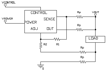
SMS1505. The advantages of remote sensing are illustrated in figures 1 through 3. Figure 1 shows the device connected
as a conventional 3 terminal regulator with the Sense lead connected directly to the output of the device. RP is the
parasitic resistance of the connections between the device and the load. Typically RP is made up of the PC traces and
/or connector resistances (in the case of a modular regulator) between the regulator and the load. Trace A of figure 3
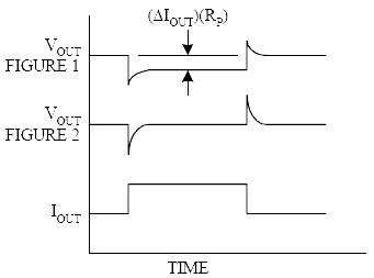
illustrates the effect of RP. Very small resistances cause significant load regulation steps. Figure 2 shows the device
connected to take advantage of the remote sense feature. The Sense pin and the top of the resistor divider are
connected to the top of the load; the bottom of the resistor divider is connected to the bottom of the load. RP is now
connected inside the regulation loop of the SMS1505 and for reasonable values of RP the load regulation at the load
will be negligible. The effect on output regulation can be seen in trace B of figure 3. Voltage drops due to RP are not
eliminated; they will add to the dropout voltage of the regulator regardless of whether they are inside or outside the
regulation loop. The SMS1505 can control the voltage at the load as long as the input-output voltage is greater than
the total of the dropout voltage of the device plus the voltage drop across RP. Stability The circuit design used in
the SMS1505 series requires the use of an output capacitor as part of the device frequency compensation. The addition
of 150µF aluminum electrolytic or a 22µF solid tantalum on the output will ensure stability for all operating
conditions. For best frequency response use capacitors with an ESR of less than 1?. In order to meet the transient
requirements of the load larger value capacitors are needed. Tight voltage tolerances are required in the power supply.
To limit the high frequency noise generated by the load high quality bypass capacitors must be used. In order to limit
parasitic inductance (ESL) and resistance (ESR) in the capacitors to acceptable limits, multiple small ceramic
capacitors in addition to high quality solid tantalum capacitors are required. When the adjustment terminal is bypassed
to improve the ripple rejection, the requirement for an output capacitor increases. The Adjust pin is brought out on
the fixed voltage device specifically to allow this capability. To ensure good transient response with heavy load
current changes capacitor values on the order of 100µF are used in the output of many regulators. To further improve
stability and transient response of these devices larger values of output capacitor can be used. The modern systems
generate large high frequency current transients. The load current step contains higher order frequency components than
the output coupling network must handle until the regulator throttles to the load current level. Because they contain
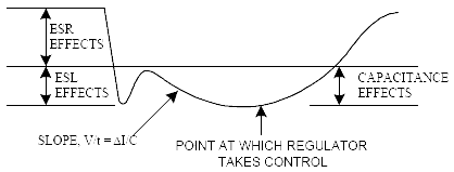
parasitic resistance and inductance, capacitors are not ideal elements. These parasitic elements dominate the change in
output voltage at the beginning of a transient load step change. The ESR of the output capacitors produces an
instantaneous step in output voltage (ΔV=ΔI)(ESR). The ESL of the output capacitors produces a droop proportional to
the rate of change of the output current (V=L)(ΔI/Δt). The output capacitance produces a change in output voltage
proportional to the time until the regulator can respond (ΔV=Δt) (ΔI/C). Figure 4 illustrates these transient effects.
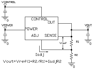
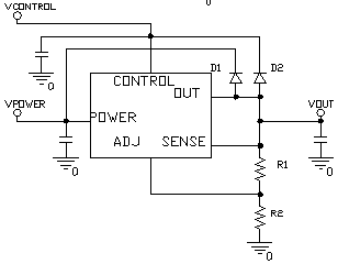
Output Voltage The SMS1505 series develops a 1.25V reference voltage between the Sense pin and the Adjust pin
(Figure5). Placing a resistor between these two terminals causes a constant current to flow through R1 and down through
R2 to set the overall output voltage. In general R1 is chosen so that this current is the specified minimum load
current of 10mA.The current out of the Adjust pin is small, typically 50?A and it adds to the current from R1. Because
IADJ is very small it needs to be considered only when very precise output voltage setting is required. For best
regulation the top of the resistor divider should be connected directly to the Sense pin. Protection Diodes Unlike
older regulators, the SMS1505 family does not need any protection diodes between the adjustment pin and the output and
from the output to the input to prevent die over-stress. Internal resistors are limiting the internal current paths on
the SMS1505 adjustment pin, therefore even with bypass capacitors on the adjust pin no protection diode is needed to
ensure device safety under short-circuit conditions. The Adjust pin can be driven on a transient basis ±7V with respect
to the output without any device degradation. Diodes between the Output pin and VPOWER pin are not usually needed.
Microsecond surge currents of 25A to 50A can be handled by the internal diode between the Output pin and VPOWER pin of
the device. In normal operations it is difficult to get those values of surge currents even with the use of large
output capacitances. If high value output capacitors are used, such as 1000µF to 5000µF and the VPOWER pin is
instantaneously shorted to ground, damage can occur. A diode from output to input is recommended, when a crowbar
circuit at the input of the SMS1505 is used (Figure 6). Normal power supply cycling or even plugging and unplugging in
the system will not generate current large enough to do any damage. If the SMS1505 is connected as a single supply
device with the control and power input pins shorted together the internal diode between the output and the power input
pin will protect the control input pin. As with any IC regulator, none the protection circuitry will be functional and
the internal transistors will break down if the maximum input to output voltage differential is exceeded. Thermal
Considerations The SMS1505 series have internal power and thermal limiting circuitry designed to protect the device
under overload conditions. However maximum junction temperature ratings should not be exceeded under continuous normal
load conditions. Careful consideration must be given to all sources of thermal resistance from junction to ambient,
including junction-to-case, case-to-heat sink interface and heat sink resistance itself. Thermal resistance
specification for both the Control Section and the Power Transistor are given in the electrical characteristics. The
thermal resistance of the Control section is given as 0.65°C/W and junction temperature of the Control section can run
up to 125°C. The thermal resistance of the Power section is given as 2.7°C/W and junction temperature of the Power
section can run up to 150°C. Due to the thermal gradients between the power transistor and the control circuitry there
is a significant difference in thermal resistance between the Control and Power sections. Virtually all the power
dissipated by the device is dissipated in the power transistor. The temperature rise in the power transistor will be
greater than the temperature rise in the Control section making the thermal resistance lower in the Control section. At
power levels below 12W the temperature gradient will be less than 25°C and the maximum ambient temperature will be
determined by the junction temperature of the Control section. This is due to the lower maximum junction temperature in
the Control section. At power levels above 12W the temperature gradient will be greater than 25°C and the maximum
ambient temperature will be determined by the Power section. In both cases the junction temperature is determined by
the total power dissipated in the device. For most low dropout applications the power dissipation will be less than
12W. The power in the device is made up of two components: the power in the output transistor and the power in the
drive circuit. The power in the control circuit is negligible. The power in the drive circuit is equal to: PDRIVE =
(VCONTROL - VOUT)(ICONTROL) where ICONTROL is equal to between IOUT/100(typ) and IOUT/58(max). The power in the output
transistor is equal to: POUTPUT = (VPOWER -VOUT)(IOUT) The total power is equal to: PTOTAL = PDRIVE + POUTPUT
Junction-to-case thermal resistance is specified from the IC junction to the bottom of the case directly below the die.
This is the lowest resistance path for the heat flow. In order to ensure the best possible thermal flow from this area
of the package to the heat sink proper mounting is required. Thermal compound at the case-to-heat sink interface is
recommended. A thermally conductive spacer can be used, if the case of the device must be electrically isolated, but
its added contribution to thermal resistance has to be considered. Conventional Load Sensing Figure 1: Conventional
Load Sensing Remote Load Sensing Figure 2: Remote Load Sensing Remote Sensing Improves Load Regulation Figure 3: Remote
Sensing Improves Load Regulation Stability and ESR effects Figure 4: Stability and ESR effects Setting Output Voltage
Figure 5: Setting Output Voltage Optional Clamp Diodes Protect Against Input Crowbar Circuits Figure 6: Optional Clamp
Diodes Protect Against Input Crowbar Circuits SEMICONDUCTOR ASSEMBLY PROCESS - SHORT APPLICATION NOTE SMX-nDFN -
NanoDFN package is a very thin (10mils) proprietary wafer level chip size package W-CSP technology developed by
Semiconix. SMX-nDFN is the most efficient wafer level chip size package W-CSP designed for mixed surface mount and flip
chip applications. The assembly process is same as for packaged surface mount components. The process consist of at
least 3 steps; -screen print solder paste on the printed circuit board; -flip chip, align and attach to the tacky
solder paste; -dry paste, reflow at >220°C, clean, etc. SMX-nDFN packages can also be attached with conductive silver
epoxy in low temperature applications. The assembly process is also very simple and inexpensive consisting of 3 steps:
- transfer a thin conductive epoxy layer onto the bonding pads; -align to substrate and attach; -cure silver epoxy and
inspect. SMX-nDFN packages are available in many sizes with landing pads compatible with the industry standard CSP as
well as many surface mount packages. STANDARD PRODUCTS ORDERING INFORMATION VERSION SMX P/N WAFFLE PACKS QUANTITY
U/P($) TAPE / REEL MIN QUANTITY U/P($) nDFN-4 SMS1505CTV-3.5V-nDFN-4 -WP 1000 -TR 1000 nDFN-4 SMS1505CTV-3.5V-nDFN-4
-WP 5000 -TR 5000 TO220-5L SMS1505CTV-3.5V-TO220-5L -WP 1000 -TR 5000 PRICES - Listed prices are only for standard
products, available from stock. Inventory is periodically updated. List prices for other quantities and tolerances are
available on line through Instant Quote. For standard products available from stock, there is a minimum line item order
of $550.00. No rights can be derived from pricing information provided on this website. Such information is indicative
only, for budgetary use only and subject to change by SEMICONIX SEMICONDUCTOR at any time and without notice. LEAD
TIMES - Typical delivery for standard products is 4-6 weeks ARO. For custom devices consult factory for an update on
minim orders and lead times. CONTINOUS SUPPLY - Semiconix guarantees continuous supply and availability of any of its
standard products provided minimum order quantities are met. CUSTOM PRODUCTS - For custom products sold as tested, bare
die or known good die KGD, there will be a minimum order quantity MOQ. Dice are 100% functional tested, visual
inspected and shipped in antistatic waffle packs. For high volume and pick and place applications, dice are also
shipped on film frame -FF. For special die level KGD requirements, different packaging or custom configurations,
contact sales via CONTACTS page. SAMPLES - Samples are available only for customers that have issued firm orders
pending qualification of product in a particular application. ORDERING - Semiconix accepts only orders placed on line
by registered customers. On line orders are verified, accepted and acknowledged by Semiconix sales department in
writing. Accepted orders are non cancelable binding contracts. SHIPING - Dice are 100% functional tested, visual
inspected and shipped in antistatic waffle packs. For high volume and pick and place applications, dice are also
shipped on film frame -FF. INSTANT QUOTE Semiconix P/N Quantity E-mail DISCLAIMER - SEMICONIX has made every effort to
have this information as accurate as possible. However, no responsibility is assumed by SEMICONIX for its use, nor for
any infringements of rights of third parties, which may result from its use. SEMICONIX reserves the right to revise the
content or modify its product line without prior notice. SEMICONIX products are not authorized for and should not be
used within support systems, which are intended for surgical implants into the body, to support or sustain life, in
aircraft, space equipment, submarine, or nuclear facility applications without the specific written consent. HOME
PRODUCT TREE PACKAGES PDF VERSION SEARCH SEMICONIX SEMICONDUCTOR www.semiconix-semiconductor.com
Tel:(408)986-8026 Fax:(408)986-8027 SEMICONIX SEMICONDUCTOR Last updated:January 01, 1970 Display settings for best
viewing: Current display settings: Page hits: 1 Screen resolution: 1124x864 Screen resolution: Total site visits: 1
Color quality: 16 bit Color quality: bit © 1990-2009 SEMICONIX SEMICONDUCTOR All rights reserved. No material from this
site may be used or reproduced without permission.
|